

Produsen Custom Global, Integrator, Consolidator, Mitra Outsourcing kanggo Macem-macem Produk & Layanan.
Kita minangka sumber siji-mandeg kanggo manufaktur, fabrikasi, teknik, konsolidasi, integrasi, outsourcing produk & layanan sing digawe khusus lan ora kasedhiya. Kita uga label pribadi / label putih produk sampeyan kanthi jeneng merek yen sampeyan pengin.
Pilih Basa sampeyan
Manufaktur Custom Parts, Komponen, Rakitan, Produk Rampung, Mesin lan Peralatan Industri
Manufaktur Kontrak Domestik & Global
Outsourcing Produksi
Domestik, Pengadaan Global Produk Industri
Labeling pribadi / Label Putih Produk sampeyan nganggo Jeneng merek sampeyan
Product Finding & Locating Services
Desain Global lan Kemitraan Saluran
Integrasi Teknik
Layanan Teknik
Konsolidasi Global, Gudang, Logistik
Search Results
164 results found with an empty search
- Global Product Finder & Product Locator Service
Global Product Finder & Product Locator Service, AI based productor finding, AI based product locating AGS-TECH, Inc. Panjenengan Produsen Kustom Global, Integrator, Konsolidator, Mitra Outsourcing. Kita minangka sumber siji-mandeg kanggo manufaktur, fabrikasi, teknik, konsolidasi, outsourcing. Global Product Finder & Service Locator Kita Product Finder / Product Locator Service kasedhiya ing upaya kanggo cepet nemokake produk sing looking for. Kita nggunakake database supplier global sing disetujoni lan uga piranti lunak Artificial Intelligence (AI) proprietary kanggo nemokake produk sing sampeyan telusuri kanthi cepet. Product Finder / Product Locator Service mesthekake yen sampeyan nampa penawaran cepet lan karo rega paling kasedhiya. Coba deleng cara kerjane: KLIK kene Click Here if you exactly know the product you are searching KLIK kene Klik ing kene yen sampeyan sebagéyan ngerti produk sing digoleki KLIK kene Click Here if you need a custom made product Kita AGS-TECH Inc., sumber siji-mandeg kanggo manufaktur & fabrikasi & engineering & outsourcing & konsolidasi. Kita minangka integrator teknik paling maneka warna ing Donya sing nawakake manufaktur, subassembly, perakitan produk lan layanan teknik khusus.
- System Components Pneumatics Hydraulics Vacuum, Booster Regulators
System Components Pneumatics Hydraulics Vacuum, Booster Regulators, Sensors Gauges, Pneumatic Cylinder Controls, Silencers, Exhaust Cleaners, Feedthroughs Komponen Sistem kanggo Pneumatik & Hidrolik lan Vakum We also supply other pneumatic, hydraulic and vacuum system components not mentioned elsewhere here under any menu page. These are: BOOSTER REGULATORS: They save money and energy by increasing the main line pressure by multiple times while also protecting downstream systems from pressure fluctuations. The pneumatic booster regulator, when connected to an air supply line, multiplies pressure and the main air supply pressure may be set low. Desired pressure increases and output pressures can be easily adjusted. Pneumatic booster regulators boost local line pressures without requiring additional power by 2 to 4 times. The use of pressure boosters is particularly recommended when the pressure in a system needs to be selectively increased. A system or sections of it do not have to be supplied with excessively high pressure, because this would lead to substantially higher operating costs. Pressure boosters can also be used for mobile pneumatics. An initial low pressure can be generated using relatively small compressors, and then reinforced with the help of the booster. Keep in mind however that pressure boosters are not a replacement for compressors. Some of our pressure boosters require no other source than compressed air. Pressure boosters are classified as twin-piston pressure boosters and are intended for compressing air. The basic variant of the booster consists of a double piston system and a directional control valve for continuous operation. These boosters double the input pressure automatically. It is not possible to adjust the pressure to lower values. Pressure boosters which also have a pressure regulator can boost pressures to less than double the set value. In this case the pressure regulator reduces the pressure in the outside chambers. Pressure boosters cannot vent themselves, the air can only flow in one direction. Therefore pressure boosters cannot necessarily be used in a working line between valves and cylinders. SENSORS and GAUGES (pressure, vacuum….etc): Your pressure, vacuum range, fluid flow range temperature range….etc. will determine which instrument to select. We have a wide range of standard off-shelf sensors and gauges for pneumatics, hydraulics and vacuum. Capacitance Manometers, Pressure Sensors, Pressure Switches, Pressure Control Subsystems, Vacuum & Pressure Gauges, Vacuum & Pressure Transducers, Indirect Vacuum Gauge Transducers & Modules and Vacuum & Pressure Gauge Controllers are some of the popular products. To select the right pressure sensor for a specific application, besides the pressure range, the type of pressure measurement has to be considered. Pressure sensors measure a certain pressure in comparison to a reference pressure and can be categorized into 1.) Absolute 2.) gage and 3.) differential devices. Absolute piezoresistive pressure sensors measure the pressure relative to a high vacuum reference sealed behind its sensing diaphragm (in practice referred to as Absolute Pressure). The vacuum is negligible compared to the pressure to be measured. Gage Pressure is measured relative to the ambient atmospheric pressure. Changes in the atmospheric pressure due to weather conditions or altitude influence the output of a gage pressure sensor. A gage pressure higher than ambient pressure is referred to as positive pressure. If the gage pressure is below the atmospheric pressure, it is called negative or vacuum gage pressure. According to its quality, vacuum can be categorized into different ranges such as low, high and ultra high vacuum. Gage pressure sensors only offer one pressure port. The ambient air pressure is directed through a vent hole or a vent tube to the back side of the sensing element and thus compensated. Differential pressure is the difference between any two process pressures p1 and p2. Because of this, differential pressure sensors must offer two separate pressure ports with connections. Our amplified pressure sensors are able to measure positive and negative pressure differences, corresponding to p1>p2 and p1p2) and the higher pressure has to be applied to the pressure port defined as ''high pressure port''. Another class of gauges available are Flow Meters. Systems requiring continuous monitoring of flow use in general electronic flow sensors rather than flow meters, which require no power. Electronic flow sensors can use a variety of sensing elements to generate an electronic signal proportional to the flow. The signal is then sent to an electronic display panel or control circuit. However, flow sensors produce no visual indication of flow by themselves, and they need some source of external power to transmit a signal to an analog or digital display. Self-contained flow meters, on the other hand, rely on the dynamics of flow to provide a visual indication of it. Flow meters operate on the principle of dynamic pressure. Because measured flow depends on fluid dynamics, changes in a fluid's physical properties can affect flow readings. This is due to the fact that a flow meter is calibrated to a fluid having a certain specific gravity within a range of viscosities. Wide variations in temperatures can change a hydraulic fluid's specific gravity and viscosity. Therefore when a flow meter is used when the fluid is very hot or very cold, flow readings may not conform to manufacturers' specifications. Other products include Temperature Sensors and Gauges. PNEUMATIC CYLINDER CONTROLS: Our speed controls have built in one-touch fittings minimizing installation time, reducing mounting height and enabling compact machine design. Our speed controls allow the body to be rotated to facilitate simple installation. Available in thread sizes in both inch and metric, with varying tube sizes, with optional elbow and universal style for increased flexibility, our speed controls are designed to meet most applications. There are several methods to control the extending and retracting speed of pneumatic cylinders. We offer Flow Controls, Speed Control mufflers, Quick Exhaust Valves for speed control. Double-acting cylinders can have both the out and in stroke controlled, and you can have several different control methods on each port. CYLINDER POSITION SENSORS: These sensors are used for the detection of magnet-equipped pistons on pneumatic and other types of cylinders. The magnetic field of a magnet embedded in the piston is detected by the sensor through the cylinder housing wall. These non-contact sensors determine the position of the cylinder piston without diminishing the integrity of the cylinder itself. These position sensors operate without intruding upon the cylinder, keeping the system completely intact. SILENCERS / EXHAUST CLEANERS: Our silencers are extremely effective in reducing air exhaust noise originating from pumps and other pneumatic devices. Our silencers reduce noise levels by up to 30dB while allowing high flow rates with minimal back pressure. We have filters that enable direct exhaust of air in a clean room. Air can be directly exhausted in a clean room only by mounting these exhaust cleaners to the pneumatic equipment in the clean room. There is no need for piping for exhaust and relief air. Product reduces piping installation work and space. FEEDTHROUGHS: These are generally electrical conductors or optical fibers used to carry a signal through an enclosure, chamber, vessel or interface. Feedthroughs can be divided into power and instrumentation categories. Power feedthroughs carry either high currents or high voltages. Instrumentation feedthroughs on the other hand are used to carry electrical signals, such as thermocouples, which are generally low current or voltage. Lastly, RF-feedthroughs are designed to carry very high frequency RF or microwave electrical signals. A feedthrough electrical connection may have to withstand considerable pressure difference across its length. Systems that operate under high vacuum, like vacuum chambers require electrical connections through the vessel. Submersible vehicles also require feedthrough connections between exterior instruments and devices and the controls within the vehicle pressure hull. Hermetically sealed feedthroughs are frequently used for instrumentation, high amperage and voltage, coaxial, thermocouple and fiber optic applications. Fiber optic feedthroughs transmit fiber optical signals through the interfaces. Mechanical feedthroughs transmit mechanical motion from one side of the interface (for example from the outside of the pressure chamber) to the other side (to the inside of the pressure chamber). Our feedthroughs incorporate ceramic, glass, metal / metal alloy parts, metal coatings on fibers for solderability and specialty silicones and epoxies, all chosen carefully according to the application. All our feedthrough assemblies have passed rigorous tests including environmental cycling test and related industrial standards. VACUUM REGULATORS: These devices assure that the vacuum process remains stable even through wide variations in flow rate and supply pressures. Vacuum regulators directly control vacuum pressures by modulating the flow from the system to the vacuum pump. Using our precision vacuum regulators is relatively simple. You simply connect your vacuum pump or vacuum utililty to the Outlet port. You connect the process you want to control to the Inlet port. By adjusting the vacuum knob you achieve the desired vacuum level. Please click on highlighted text below to download our product brochures for pneumatic & hydraulic & vacuum system components: - Pneumatic Cylinders - Private Label Gauges, Filters, Regulators, Temperature Instruments (We private label these with your brand name and logo if you wish) - Private Label Pneumatic Compressed Air Hoses Fittings (We private label these with your brand name and logo if you wish) - Private Label Pneumatic Couplings, Plugs and Nipples (We private label these with your brand name and logo if you wish) - Process Automation Solutions (We private label these with your brand name and logo if you wish) - YC Series Hydraulic Cyclinder - Accumulators from AGS-TECH Inc - Information on our facility producing ceramic to metal fittings, hermetic sealing, vacuum feedthroughs, high and ultrahigh vacuum and fluid control components can be found here: Fluid Control Factory Brochure KLIK Product Finder-Locator Service PAGE sadurunge
- Hole Saws & Hole Saw, Albuquerque USA, AGS-TECH Inc.
High quality Hole Saws & Hole Saw for cutting different materials. We have hole saws made from various materials to cut wood, masonry, glass and more. Saws bolongan Mangga klik teks sing disorot ing produk hole saw ing ngisor iki kanggo ngundhuh brosur sing gegandhengan. We do duwe spektrum sudhut saws bolongan cocok kanggo meh kabeh aplikasi. Ana macem-macem saka sudhut saws bolongan karo dimensi beda, aplikasi lan materi; mokal kanggo nampilake kabeh ing kene. Yen sampeyan ora bisa nemokake utawa yen sampeyan ora yakin kang bolongan saws bakal ketemu pangarepan lan syarat, email utawa nelpon kita supaya kita bisa nemtokake produk sing paling pas kanggo sampeyan. Nalika ngubungi kita, coba wenehi kanthi rinci kayata aplikasi, dimensi, bahan bahan yen sampeyan ngerti, syarat finishing, syarat kemasan & label lan mesthi jumlah pesenan sing direncanakake. Bi-metal Hole Saws Diamond Brazed Hole Saw Carbide Grit Hole Saws HSS Hole Saws Woodworking Hole Saws Diamond Hole Saws TCT Hole Saws HSS JetBroach Cutters TCT JetBroach Cutters Baja Karbon Hole Saws Luwes Luwes Cutter Diamond Core Drill Bits Mata Bor Inti TCT Ubin & Kaca Bit Private Label Power Tool Accessories Brosur iki kalebu sawetara saws bolongan. Kita bisa menehi label pribadi alat tangan iki yen sampeyan pengin. Ing tembung liyane, kita bisa nyelehake jeneng perusahaan, merek lan label. Kanthi cara iki sampeyan bisa promosi merek kanthi adol maneh menyang pelanggan. KLIK kene kanggo ngundhuh kemampuan teknis lan pandhuan referensi kanggo nglereni, ngebur, grinding, mbentuk, mbentuk, alat polishing sing digunakake ing medis, dental, instrumentasi presisi, stamping logam, die forming lan aplikasi industri liyane. KLIK Product Finder-Locator Service Klik kene kanggo pindhah menyang Cut, Drilling, Grinding, Lapping, Polishing, Dicing lan Shaping Tools Menu Ref. Kode: OICASOSTAR
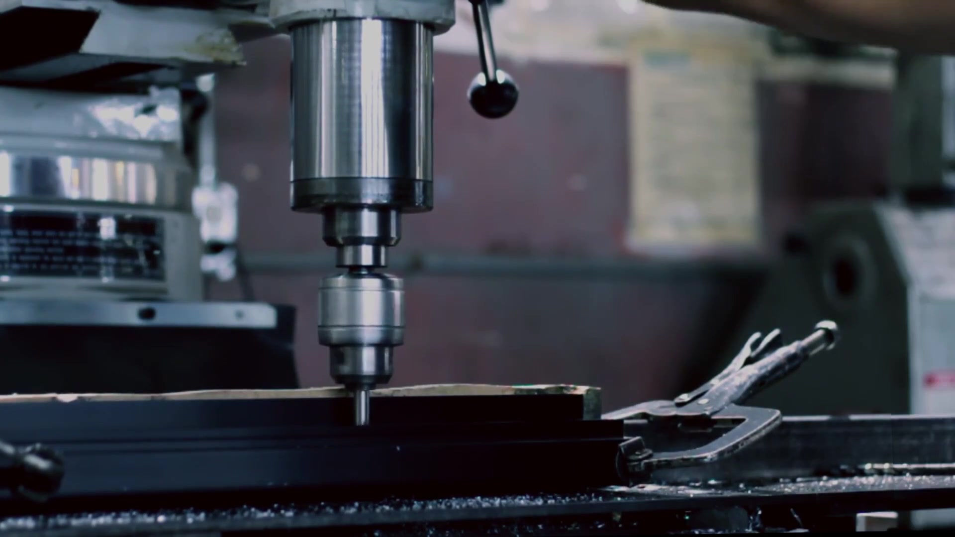
- Casting and Machined Parts, CNC Manufacturing, Milling, Turning, Swiss
Casting and Machined Parts, CNC Manufacturing, Milling, Turning, Swiss Type Machining, Die Casting, Investment Casting, Lost Foam Cast Parts from AGS-TECH Inc. Casting lan Machining Our custom casting and machining techniques are expendable and non-expendable castings, ferrous and nonferrous casting, sand, die, centrifugal, continuous, ceramic mold, investment, lost foam, near-net-shape, permanent mold (gravity die casting), plaster mold (plaster casting) and shell castings, machined parts produced by milling and turning using conventional as well as CNC equipment, swiss type machining for high throughput inexpensive small precision parts, screw machining for fasteners, non-conventional machining. Please keep in mind that besides metals and metal alloys, we machine ceramic, glass and plastic components as well in some cases when manufacturing a mould is not appealing or not the option. Machining of polymer materials requires the specialized experience we have because of the challenge plastics and rubber presents due to their softness, non-rigidity...etc. For machining of ceramic and glass, please see our page on Non-Conventional Fabrication. AGS-TECH Inc. manufactures and supplies both lightweight and heavy castings. We have been supplying metal castings and machined parts for boilers, heat exchangers, automobiles, micromotors, wind turbines, food packaging equipment and more. We recommend that you click here to DOWNLOAD our Schematic Illustrations of Machining and Casting Processes by AGS-TECH Inc. This will help you better understand the information we are providing you below. Let’s look at some of the various techniques we offer in detail: • EXPENDABLE MOLD CASTING : This broad category refers to methods that involve temporary and non-reusable molds. Examples are sand, plaster, shell, investment (also called lost-wax) and plaster casting. • SAND CASTING : A process where sand is used as the mold material. A very old method and still very popular to the extent that the majority of metal castings produced are made by this technique . Low cost even at low quantity production. Suitable for small and large parts manufacturing. The technique can be used to manufacture parts within days or weeks with very little investment. The moist sand is bonded together using clay, binders or special oils. Sand is generally contained in mold boxes and cavity & gate system are created by compacting the sand around models. The processes are: 1.) Placing of the model in sand to make the mold 2.) Incorporation of model and sand in a gating system 3.) Removal of model 4.) Filling of mold cavity with molten metal 5.) Cooling of the metal 6.) Breaking the sand mold and removal of the casting • PLASTER MOLD CASTING : Similar to sand casting, and instead of sand, plaster of paris is being used as the mold material. Short production lead times like sand casting and inexpensive. Good dimensional tolerances and surface finish. Its major disadvantage is that it can only be used with low melting point metals like aluminum and zinc. • SHELL MOLD CASTING : Also similar to sand casting. Mold cavity obtained by hardened shell of sand and thermosetting resin binder instead of flask filled with sand as in sand casting process. Almost any metal suitable to be cast by sand can be cast by shell molding. The process can be summarized as: 1.) Manufacturing of the shell mold. Sand used is of a much smaller grain size when compared to sand used in sand casting. The fine sand is mixed with thermosetting resin. The metal pattern is coated with a parting agent to make removal of the shell easier. Thereafter the metal pattern is heated and the sand mixture is pored or blown onto the hot casting pattern. A thin shell forms on the surface of the pattern. The thickness of this shell can be adjusted by varying the length of time the sand resin mixture is in contact with the metal pattern. The loose sand is then removed with the shell covered pattern remaining. 2.) Next, the shell and pattern are heated in an oven so that the shell hardens. After hardening is complete, the shell is ejected from pattern using pins built into the pattern. 3.) Two such shells are assembled together by gluing or clamping and make up the complete mold. Now the shell mold is inserted into a container in which it is supported by sand or metal shot during the casting process. 4.) Now the hot metal can be poured into the shell mold. Advantages of shell casting are products with very good surface finish, possibility of manufacturing complex parts with high dimensional accuracy, process easy to automate, economical for large volume production. Disadvantages are the molds necessitate good ventilation because of gases that are created when molten metal contacts the binder chemical, the thermosetting resins and metal patterns are expensive. Due to the cost of metal patterns, the technique may not suit well for low quantity production runs. • INVESTMENT CASTING ( also known as LOST-WAX CASTING ): Also a very old technique and suitable for manufacturing quality parts with high accuracy, repeatability, versatility and integrity from many metals, refractory materials and special high performance alloys. Small as well as large sized parts can be produced. An expensive process when compared to some of the other methods, but major advantage is the possibility to produce parts with near net shape, intricate contours and details. So the cost is somewhat offset by the elimination of rework and machining in some cases. Even though there can be variations, here is a summary of the general investment casting process: 1.) Creation of original master pattern from wax or plastic. Each casting needs one pattern as these are destroyed in the process. Mold from which patterns are manufactured is also needed and most of the time the mold is cast or machined. Because the mold does not need to be opened, complex castings can be achieved, many wax patterns can be connected like the branches of a tree and poured together, thus enabling production of multiple parts from a single pouring of the metal or metal alloy. 2.) Next, the pattern is dipped or poured over with a refractory slurry composed of very fine grained silica, water, binders. This results in a ceramic layer over the surface of the pattern. The refractory coat on pattern is left to dry and harden. This step is where the name investment casting comes from: Refractory slurry is invested over the wax pattern. 3.) At this step, the hardened ceramic mould is turned upside down and heated so that the wax melts and pours out of the mould. A cavity is left behind for the metal casting. 4.) After the wax is out, the ceramic mold is heated to even a higher temperature which results in strengthening of the mold. 5.) Metal casting is poured into the hot mold filling all intricate sections. 6.) Casting is allowed to solidify 7.) Finally the ceramic mould is broken and manufactured parts are cut from the tree. Here is a link to Investment Casting Plant Brochure • EVAPORATIVE PATTERN CASTING : The process uses a pattern made from a material such as polystyrene foam that will evaporate when hot molten metal is poured into the mold. There are two types of this process: LOST FOAM CASTING which uses unbonded sand and FULL MOLD CASTING which uses bonded sand. Here are the general process steps: 1.) Manufacture the pattern from a material such as polystyrene. When large quantities will be manufactured, the pattern is molded. If part has a complex shape, several sections of such foam material may need to be adhered together to form the pattern. We often coat the pattern with a refractory compound to create a good surface finish on the casting. 2.) The pattern is then put into molding sand. 3.) The molten metal is poured into the mould, evaporating the foam pattern, i.e. polystyrene in most cases as it flows through the mold cavity. 4.) The molten metal is left in the sand mold to harden. 5.) After it is hardened, we remove the casting. In some cases, the product we manufacture requires a core within the pattern. In evaporative casting, there is no need to place and secure a core in the mold cavity. The technique is suitable for manufacturing of very complex geometries, it can be easily automated for high volume production, and there are no parting lines in the cast part. The basic process is simple and economical to implement. For large volume production, since a die or mold is needed to produce the patterns from polystyrene, this may be somewhat costly. • NON-EXPANDABLE MOLD CASTING : This broad category refers to methods where the mold does not need to be reformed after each production cycle. Examples are permanent, die, continuous and centrifugal casting. Repeatability is obtained and parts can be characterized as NEAR NET SHAPE. • PERMANENT MOLD CASTING : Reusable molds made from metal are used for multiple castings. A permanent mold can generally be used for tens of thousands of times before it wears out. Gravity, gass pressure or vacuum are generally used to fill the mould. Molds (also called die) is generally made of iron, steel, ceramic or other metals. The general process is: 1.) Machine and create the mould. It is common to machine the mold out of two metal blocks that fit together and can be opened and closed. Both the part features as well as the gating system is generally machined into the casting mould. 2.) The internal mold surfaces are coated with a slurry incorporating refractory materials. This helps to control heat flow and acts as a lubricant for easy removal of the cast part. 3.) Next, the permanent mold halves are closed and the mold is heated. 4.) Molten metal is poured into mould and let still for solidification. 5.) Before much cooling occurs, we remove the part from permanent mold using ejectors when mold halves are opened. We frequently use permanent mold casting for low melting point metals such as zinc and aluminum. For steel castings, we use graphite as mold material. We sometimes obtain complex geometries using cores within permanent molds. Advantages of this technique are castings with good mechanical properties obtained by rapid cooling, uniformity in properties, good accuracy and surface finish, low reject rates, possibility of automating the process and producing high volumes economically. Disadvantages are high initial setup costs which make it unsuitable for low volume operations, and limitations on the size of the parts manufactured. • DIE CASTING : A die is machined and molten metal is pushed under high pressure into mold cavities. Both nonferrous as well as ferrous metal die castings are possible. The process is suitable for high quantity production runs of small to medium sized parts with details, extremely thin walls, dimensional consistency and good surface finish. AGS-TECH Inc. is capable to manufacture wall thicknesses as small as 0.5 mm using this technique. Like in permanent mold casting, the mold needs to consist of two halves that can open and close for removal of part produced. A die casting mold may have multiple cavities to enable production of multiple castings with each cycle. Die casting molds are very heavy and much larger than the parts they produce, therefore also expensive. We repair and replace worn out dies free of charge for our customers as long as they reorder their parts from us. Our dies have long lifetimes in the several hundred thousand cycles range. Here are the basic simplified process steps: 1.) Production of the mold generally from steel 2.) Mold installed on die casting machine 3.) The piston forces molten metal to flow in the die cavities filling out the intricate features and thin walls 4.) After filling the mold with the molten metal, the casting is let hardened under pressure 5.) Mold is opened and casting removed with the help of ejector pins. 6.) Now the empty die are lubricated again and are clamped for the next cycle. In die casting, we frequently use insert molding where we incorporate an additional part into the mold and cast the metal around it. After solidification, these parts become part of the cast product. Advantages of die casting are good mechanical properties of the parts, possibility of intricate features, fine details and good surface finish, high production rates, easy automation. Disadvantages are: Not very suitable for low volume because of high die and equipment cost, limitations in shapes that can be cast, small round marks on cast parts resulting from contact of ejector pins, thin flash of metal squeezed out at the parting line, need for vents along the parting line between the die, necessity to keep mold temperatures low using water circulation. • CENTRIFUGAL CASTING : Molten metal is poured into the center of the rotating mold at the axis of rotation. Centrifugal forces throw the metal towards the periphery and it is let to solidify as the mold keeps rotating. Both horizontal and vertical axis rotations can be used. Parts with round inner surfaces as well as other non-round shapes can be cast. The process can be summarized as: 1.) Molten metal is poured into centrifugal mould. The metal is then forced to the outer walls due to spinning of the mold. 2.) As the mold rotates, the metal casting hardens Centrifugal casting is a suitable technique for production of hollow cylindirical parts like pipes, no need for sprues, risers and gating elements, good surface finish and detailed features, no shrinkage issues, possibility to produce long pipes with very large diameters, high rate production capability. • CONTINUOUS CASTING ( STRAND CASTING ) : Used to cast a continuous length of metal. Basically the molten metal is cast into two dimensional profile of the mold but its length is indeterminate. New molten metal is constantly fed into the mould as the casting travels downward with its length increasing with time. Metals such as copper, steel, aluminum are cast into long strands using continuous casting process. The process may have various configurations but the common one can be simplified as: 1.) Molten metal is poured into a container located high above the mold at well calculated amounts and flow rates and flows through the water cooled mold. The metal casting poured into the mould solidifies to a starter bar placed at the bottom of the mold. This starter bar gives the rollers something to grab onto initially. 2.) The long metal strand is carried by rollers at a constant speed. The rollers also change the direction of the flow of metal strand from vertical to horizontal. 3.) After the continuous casting has travelled a certain horizontal distance, a torch or saw that moves with the casting quickly cuts it to desired lengths. Continuous casting process can be integrated with ROLLING PROCESS, where the continuously cast metal can be fed directly into a rolling mill to produce I-Beams, T-Beams….etc. Continuous casting produces uniform properties throughout the product, it has a high solidification rate, reduces cost due to very low loss of material, offers a process where loading of metal, pouring, solidification, cutting and casting removal all take place in a continuous operation and thus resulting in high productivity rate and high quality. A major consideration is however the high initial investment, setup costs and space requirements. • MACHINING SERVICES : We offer three, four and five - axis machining. The type of machining processes we use are TURNING, MILLING, DRILLING, BORING, BROACHING, PLANING, SAWING, GRINDING, LAPPING, POLISHING and NON-TRADITIONAL MACHINING which is further elaborated under a different menu of our website. For most of our manufacturing, we use CNC machines. However for some operations conventional techniques are a better fit and therefore we rely on them as well. Our machining capabilities reach the highest level possible and some most demanding parts are manufactured at an AS9100 certified plant. Jet engine blades require highly specialized manufacturing experience and the right equipment. Aerospace industry has very strict standards. Some components with complex geometrical structures are most easily manufactured by five axis machining, which is found only in some machining plants including ours. Our aerospace certified plant has the necessary experience complying to extensive documentation requirement of the aerospace industry. In TURNING operations, a workpiece is rotated and moved against a cutting tool. For this process a machine called lathe is being used. In MILLING, a machine called milling machine has a rotating tool to bring cutting edges to bear against a workpiece. DRILLING operations involve a rotating cutter with cutting edges that produces holes upon contact with the workpiece. Drill presses, lathes or mills are generally used. In BORING operations a tool with a single bent pointed tip is moved into a rough hole in a spinning workpiece to slightly enlarge the hole and improve accuracy. It is used for fine finishing purposes. BROACHING involves a toothed tool to remove material from a workpiece in one pass of the broach (toothed tool). In linear broaching, the broach runs linearly against a surface of the workpiece to effect the cut, whereas in rotary broaching, the broach is rotated and pressed into the workpiece to cut an axis symmetric shape. SWISS TYPE MACHINING is one of our valuable techniques we use for high volume manufacturing of small high precision parts. Using Swiss-type lathe we turn small, complex, precision parts inexpensively. Unlike conventional lathes where the workpiece is kept stationary and tool moving, in Swiss-type turning centers, the workpiece is allowed to move in the Z-axis and the tool is stationary. In Swiss-type machining, the bar stock is held in the machine and advanced through a guide bushing in the z-axis, only exposing the portion to be machined. This way a tight grip is ensured and accuracy is very high. Availability of live tools provide the opportunity to mill and drill as the material advances from the guide bushing. The Y-axis of the Swiss-type equipment provides full milling capabilities and saves great amount of time in manufacturing. Furthermore, our machines have drills and boring tools that operate on the part when it is held in the sub spindle. Our Swiss-Type machining capability gives us a fully automated complete machining opportunity in a single operation. Machining is one of the largest segments of AGS-TECH Inc. business. We either use it as a primary operation or a secondary operation after casting or extruding a part so that all drawing specifications are met. • SURFACE FINISHING SERVICES : We offer a vast variety of surface treatments and surface finishing such as surface conditioning to enhance adhesion, depositing thin oxide layer to enhance adhesion of coating, sand blasting, chem-film, anodizing, nitriding, powder coating, spray coating, various advanced metallization and coating techniques including sputtering, electron beam, evaporation, plating, hard coatings such as diamond like carbon (DLC) or titanium coating for drilling and cutting tools. • PRODUCT MARKING & LABELING SERVICES : Many of our customers require marking and labeling, laser marking, engraving on metal parts. If you have any such need, let us discuss which option will be the best for you. Here are some of commonly used metal cast products. Since these are off-the-shelf, you can save on mould costs in case any of these fits your requirements: CLICK HERE TO DOWNLOAD our 11 Series Die-cast Aluminium Boxes from AGS-Electronics KLIK Product Finder-Locator Service PAGE sadurunge
- Gears and Gear Drives, Gear Assembly, Spur Gears, Rack & Pinion
Gears and Gear Drives, Gear Assembly, Spur Gears, Rack & Pinion & Bevel Gears, Miter, Worms, Machine Elements Manufacturing at AGS-TECH Inc. Gear & Gear Drive Majelis AGS-TECH Inc. offers you power transmission components including GEARS & GEAR DRIVES. Gears transmit motion, rotating or reciprocating, from one machine part to another. Where necessary, gears reduce or increase the revolutions of the shafts. Basically gears are rolling cylindrical or conic-shaped components with teeth on their contact surfaces to ensure positive motion. Please note that gears are the most durable and rugged of all mechanical drives. Most heavy-duty machine drives and automobiles, transportation vehicles preferably use gears rather than belts or chains. We have many kinds of gears. - SPUR GEARS: These gears connect parallel shafts. Spur gear proportions and teeth shape are standardized. Gear drives need to be operated under a variety of conditions and therefore it is very difficult to determine the best gear set for a particular application. The easiest is to select from stocked standard gears with an adequate load rating. Approximate power ratings for spur gears of various sizes (number of teeth) at several operating speeds (revolutions/minute) are available in our catalogs. For gears with sizes and speeds not listed, ratings can be estimated from values shown on special tables and graphs. Service class and factor for spur gears is also a factor in the selection process. - RACK GEARS: These gears convert spur gears motion to reciprocating or linear motion. A rack gear is a straight bar with teeth that engage the teeth on a spur gear. The specifications for the teeth of the rack gear are given in the same manner as for spur gears, because rack gears can be imagined as spur gears having an infinite pitch diameter. Basically, all circular dimensions of spur gears become linear fir rack gears. - BEVEL GEARS (MITER GEARS and else): These gears connect shafts whose axes intersect. The axes of bevel gears may intersect at an angle, but the most common angle is 90 degrees. The teeth of bevel gears are the same shape as spur gear teeth, but taper toward the cone apex. Miter gears are bevel gears having the same diametral pitch or module, pressure angle and number of teeth. - WORMS and WORM GEARS: These gears connect shafts whose axes do not intersect. Worm gears are used to transmit power between two shafts that are at right angles to each other and are nonintersecting. Teeth on the worm gear are curved to conform with the teeth on the worm. The lead angle on worms should be between 25 and 45 degrees to be efficient in power transmission. Multi-thread worms with one to eight threads are used. - PINION GEARS: The smaller of the two gears is called pinion gear. Often a gear and pinion are made of different materials for better efficiency and durability. The pinion gear is made of a stronger material because the teeth on the pinion gear come into contact more times than the teeth on the other gear. We have standard catalog items as well the capability to manufacture gears according to your request and specifications. We also offer gear design, assembly and manufacturing. Gear design is very complicated because designers need to be dealing with problems such as strength, wear and material selection. The majority of our gears are made of cast iron, steel, brass, bronze or plastic. We have five levels of tutorial for gears, please read them in the given order. If you are not familiar with gears and gear drives, these tutorials below will help you in designing your product. If you prefer, we can also assist you in choosing the right gears for your design. Click on highlighted text below to download the relevant product catalog: - Introductory guide for gears - Basic guide for gears - Guide for practical use of gears - Introduction to gears - Technical reference guide for gears To help you compare applicable standards related to gears in different parts of the World, here you can download: Equivalency Tables for Standards of Raw Material and Gear Precision Grade Once more, we would like to repeat that in order to purchase gears from us, you do not need to have a particular part number, size of gear….etc handy. You do not need to be an expert in gears and gear drives. All you need is really to provide us as much information as possible regarding your application, dimensional limitations where the gears need to be installed, maybe photos of your system…and we will help you. We use computer software packages for the integrated design and manufacture of generalized gear pairs. These gear pairs include cylindrical, bevel, skew-axis, worm and worm wheel, along with non-circular gear pairs. The software we use is based on mathematical relations that differ from established standards and practice. This enables the following features: • any face width • any gear ratio (linear & nonlinear) • any number of teeth • any spiral angle • any shaft center distance • any shaft angle • any tooth profile. These mathematical relations seamlessly encompass different gear types to design and manufacture gear pairs. Here are some of our off-shelf gear and gear drive brochures and catalogs. Click on colored text to download: - Gears - Worm Gears - Worms and Gear Racks - Slewing Drives - Slewing Rings (some have internal or external gears) - Worm Gear Speed Reducers - WP Model - Worm Gear Speed Reducers - NMRV Model - T-Type Spiral Bevel Gear Redirector - Worm Gear Screw Jacks Reference Code: OICASKHK KLIK Product Finder-Locator Service PAGE sadurunge
- Mesomanufacturing,Mesoscale Manufacturing,Miniature Device Fabrication
Mesomanufacturing - Mesoscale Manufacturing - Miniature Device Fabrication - Tiny Motors - AGS-TECH Inc. - New Mexico Manufaktur Mesoscale / Mesomanufacturing With conventional production techniques we produce “macroscale” structures that are relatively large and visible to the naked eye. With MESOMANUFACTURING however we produce components for miniature devices. Mesomanufacturing is also referred to as MESOSCALE MANUFACTURING or MESO-MACHINING. Mesomanufacturing overlaps both macro and micromanufacturing. Examples of mesomanufacturing are hearing aides, stents, very small motors. The first approach in mesomanufacturing is to scale macromanufacturing processes down. For example a tiny lathe with dimensions in the few dozen millimeters and a motor of 1.5W weighing 100 grams is a good example of mesomanufacturing where downscaling has taken place. The second approach is to scale micromanufacturing processes up. As an example LIGA processes can be upscaled and enter the realm of mesomanufacturing. Our mesomanufacturing processes are bridging the gap between silicon-based MEMS processes and conventional miniature machining. Mesoscale processes can fabricate two and three-dimensional parts having micron size features in traditional materials such as stainless steels, ceramics, and glass. Mesomanufacturing processes that are currently available to us include, focused ion beam (FIB) sputtering, micro-milling, micro-turning, excimer laser ablation, femto-second laser ablation, and micro electro-discharge (EDM) machining. These mesoscale processes employ subtractive machining technologies (i.e., material removal), whereas the LIGA process, is an additive mesoscale process. Mesomanufacturing processes have different capabilities and performance specifications. Machining performance specifications of interest include minimum feature size, feature tolerance, feature location accuracy, surface finish, and material removal rate (MRR). We have the capability of mesomanufacturing electro-mechanical components that require mesoscale parts. The mesoscale parts fabricated by subtractive mesomanufacturing processes have unique tribological properties because of the variety of materials and the surface conditions produced by the different mesomanufacturing processes. These subtractive mesoscale machining technologies bring us concerns related to cleanliness, assembly, and tribology. Cleanliness is vital in mesomanufacturing because mesoscale dirt and debris particle size created during the meso-machining process can be comparable to mesoscale features. Mesoscale milling and turning can create chips and burrs that can block holes. Surface morphology and surface finish conditions vary greatly depending on the mesomanufacturing method. Mesoscale parts are difficult to handle and align which makes assembly a challenge which most of our competitors are unable to overcome. Our yield rates in mesomanufacturing is far higher than our competitors which gives us the advantage of being able to offer better prices. MESOSCALE MACHINING PROCESSES: Our major mesomanufacturing techniques are Focused Ion Beam (FIB), Micro-milling, & Micro-turning, laser meso-machining, Micro-EDM (electro-discharge machining) Mesomanufacturing using focused Ion Beam (FIB), Micro-milling, & Micro-turning: The FIB sputters material from a workpiece by Gallium ion beam bombardment. The workpiece is mounted to a set of precision stages and is placed in a vacuum chamber underneath the source of Gallium. The translation and rotation stages in the vacuum chamber make various locations on the work piece available to the beam of Gallium ions for FIB mesomanufacturing. A tunable electric field scans the beam to cover a pre-defined projected area. A high voltage potential causes a source of Gallium ions to accelerate and collide with the work piece. The collisions strip away atoms from the work piece. The result of the FIB meso-machining process can be the creation of a near vertical facets. Some FIBs available to us have beam diameters as small as 5 nanometers, making the FIB a mesoscale and even microscale capable machine. We mount micro-milling tools on high precision milling machines to machine channels in aluminum. Using FIB we can fabricate micro-turning tools which can then be used on a lathe to fabricate finely threaded rods. In other words, FIB can be used to machine hard tooling besides directly meso-machining features onto the end work piece. The slow material removal rate has rendered the FIB as impractical for directly machining large features. The hard tools, however, can remove material at an impressive rate and are durable enough for several hours of machining time. Nevertheless, the FIB is practical for directly meso-machining complex three dimensional shapes that do not require a substantial material removal rate. Length of exposure and angle of incidence can greatly affect the geometry of directly machined features. Laser Mesomanufacturing: Excimer lasers are used for mesomanufacturing. The excimer laser machines material by pulsing it with nanosecond pulses of ultraviolet light. The work piece is mounted to precision translational stages. A controller coordinates the motion of the work piece relative to the stationary UV laser beam and coordinates the firing of the pulses. A mask projection technique can be used to define meso-machining geometries. The mask is inserted into the expanded part of the beam where the laser fluence is too low to ablate the mask. The mask geometry is de-magnified through the lens and projected onto the work piece. This approach can be used for machining multiple holes (arrays) simultaneously. Our excimer and YAG lasers can be used to machine polymers, ceramics, glass and metals having feature sizes as small as 12 microns. Good coupling between the UV wavelength (248 nm) and the workpiece in laser mesomanufacturing / meso-machining results in vertical channel walls. A cleaner laser meso-machining approach is to use a Ti-sapphire femtosecond laser. The detectable debris from such mesomanufacturing processes are nano-sized particles. Deep one micron-size features can be microfabricated using the femtosecond laser. The femtosecond laser ablation process is unique in that it breaks atomic bonds instead of thermally ablating material. The femtosecond laser meso-machining / micromachining process has a special place in mesomanufacturing because it is cleaner, micron capable, and it is not material specific. Mesomanufacturing using Micro-EDM (electro-discharge machining): Electro-discharge machining removes material through a spark erosion process. Our micro-EDM machines can produce features as small as 25 microns. For the sinker and the wire micro-EDM machine, the two major considerations for determining feature size are the electrode size and the over-bum gap. Electrodes little over 10 microns in diameter and over-bum as little as a few microns are being used. Creating an electrode having a complex geometry for the sinker EDM machine requires know-how. Both graphite and copper are popular as electrode materials. One approach to fabricating a complicated sinker EDM electrode for a mesoscale part is to use the LIGA process. Copper, as the electrode material, can be plated into LIGA molds. The copper LIGA electrode can then be mounted onto the sinker EDM machine for mesomanufacturing a part in a different material such as stainless steel or kovar. No one mesomanufacturing process is sufficient for all operations. Some mesoscale processes are more wide reaching than others, but each process has its niche. Most of the time we require a variety of materials to optimize performance of mechanical components and are comfortable with traditional materials such as stainless steel because these materials have a long history and have been very well characterized through the years. Mesomanufacturing processes allow us to use traditional materials. Subtractive mesoscale machining technologies expand our material base. Galling may be an-issue with some material combinations in mesomanufacturing. Each particular mesoscale machining process uniquely affects the surface roughness and morphology. Micro-milling and micro-turning may generate burrs and particles that can cause mechanical problems. Micro-EDM may leave a recast layer that can have particular wear and friction characteristics. Friction effects between mesoscale parts may have limited points of contact and are not accurately modeled by surface contact models. Some mesoscale machining technologies, such as micro-EDM, are fairly mature, as opposed to others, such as femtosecond laser meso-machining, which still require additional development. KLIK Product Finder-Locator Service PAGE sadurunge
- Joining & Assembly & Fastening Processes, Welding, Brazing, Soldering
Joining & Assembly & Fastening Processes, Welding, Brazing, Soldering, Sintering, Adhesive Bonding, Press Fitting, Wave and Reflow Solder Process, Torch Furnace Proses Gabung & Majelis & Fastening We join, assemble and fasten your manufactured parts and turn them into finished or semi-finished products using WELDING, BRAZING, SOLDERING, SINTERING, ADHESIVE BONDING, FASTENING, PRESS FITTING. Some of our most popular welding processes are arc, oxyfuel gas, resistance, projection, seam, upset, percussion, solid state, electron beam, laser, thermit, induction welding. Our popular brazing processes are torch, induction, furnace and dip brazing. Our soldering methods are iron, hot plate, oven, induction, dip, wave, reflow and ultrasonic soldering. For adhesive bonding we frequently use thermoplastics and thermo-setting, epoxies, phenolics, polyurethane, adhesive alloys as well as some other chemicals and tapes. Finally our fastening processes consist of nailing, screwing, nuts and bolts, riveting, clinching, pinning, stitching & stapling and press fitting. - Screws and Fasteners (Standard and Specialty) (Click on the blue text above to download the brochure. We can private label these for you. In other words, we can put your name and logo on these products) - Screws for Furniture and Wood (Click on the blue text above to download the brochure. We can private label these for you. In other words, we can put your name and logo on these products) - Screws for Window and Door (Click on the blue text above to download the brochure. We can private label these for you. In other words, we can put your name and logo on these products) • WELDING : Welding involves joining of materials by melting the work pieces and introducing filler materials, that also joins the molten weld pool. When the area cools, we obtain a strong joint. Pressure is applied in some cases. Contrary to welding, the brazing and soldering operations involve only the melting of a material with lower melting point between the workpieces, and workpieces do not melt. We recommend that you click here to DOWNLOAD our Schematic Illustrations of Welding Processes by AGS-TECH Inc. This will help you better understand the information we are providing you below. In ARC WELDING, we use a power supply and an electrode to create an electric arc that melts the metals. Welding point is protected by a shielding gas or vapor or other material. This process is popular for welding automotive parts and steel structures. In shelded metal arc welding (SMAW) or also known as stick welding, an electrode stick is brought close to the base material and an electric arc is generated between them. The electrode rod melts and acts as the filler material. The electrode also contains flux that acts as a layer of slag and gives off vapors that act as the shielding gas. These protect the weld area from environmental contamination. No other fillers are being used. The disadvantages of this process are its slowness, need to replace electrodes frequently, the need to chip away the residual slag originating from flux. A number of metals such as iron, steel, nickel, aluminum, copper…etc. Can be welded. Its advantages are its inexpensive tools and ease of use. Gas metal arc welding (GMAW) also known as metal-inert gas (MIG), we have continuous feeding of a consumable electrode wire filler and an inert or partially inert gas that flows around the wire against environmental contamination of the weld region. Steel, aluminum and other non-ferrous metals can be welded. The advantages of MIG are high welding speeds and good quality. The disadvantages are its complicated equipment and challenges faced in windy outdoor environments because we have to maintain the shielding gas around the welding area stable. A variation of GMAW is flux-cored arc welding (FCAW) which consists of a fine metal tube filled with flux materials. Sometimes the flux inside the tube is sufficient for protection from environmental contamination. Submerged Arc Welding (SAW) widely an automated process, involves continuous wire feeding and arc that is struck under a layer of flux cover. The production rates and quality are high, welding slag comes off easily, and we have a smoke free work environment. The disadvantage is that it can only be used to weld parts in certain positions. In gas tungsten arc welding (GTAW) or tungsten-inert gas welding (TIG) we use a Tungsten electrode along with a separate filler and inert or near inert gases. As we know Tungsten has a high melting point and it is a very suitable metal for very high temperatures. The Tungsten in TIG is not consumed contrary to the other methods explained above. A slow but a high quality welding technique advantageous over other techniques in welding of thin materials. Suitable for many metals. Plasma arc welding is similar but uses plasma gas to create the arc. The arc in plasma arc welding is relatively more concentrated in comparison to GTAW and can be used for a wider range of metal thicknesses at much higher speeds. GTAW and plasma arc welding can be applied to more or less same materials. OXY-FUEL / OXYFUEL WELDING also called oxyacetylene welding, oxy welding, gas welding is carried out using gas fuels and oxygen for welding. Since no electric power is used it is portable and can be used where there is no electricity. Using a welding torch we heat the pieces and the filler material to produce a shared molten metal pool. Various fuels can be used such as acetylene, gasoline, hydrogen, propane, butane…etc. In oxy-fuel welding we use two containers, one for the fuel and the other for oxygen. The oxygen oxidizes the fuel (burns it). RESISTANCE WELDING: This type of welding takes advantage of joule heating and heat is generated at the location where electric current is applied for a certain time. High currents are passed through the metal. Pools of molten metal are formed at this location. Resistance welding methods are popular due to their efficiency, little pollution potential. However disadvantages are equipment costs being relatively significant and the inherent limitation to relatively thin work pieces. SPOT WELDING is one major type of resistance welding. Here we join two or more overlapping sheets or work pieces by using two copper electrodes to clamp the sheets together and pass a high current through them. The material between the copper electrodes heats up and a molten pool is generated at that location. The current is then stopped and the copper electrode tips cool the weld location because the electrodes are water cooled. Applying the right amount of heat to the right material and thickness is key for this technique, because if applied wrongly the joint will be weak. Spot welding has the advantages of causing no significant deformation to workpieces, energy efficiency, ease of automation and outstanding production rates, and not requiring any fillers. The disadvantage is that since welding takes place at spots rather than forming a continuous seam, the overall strength can be relatively lower as compared to other welding methods. SEAM WELDING on the other hand produces welds at the faying surfaces of similar materials. The seam can be butt or overlap joint. Seam welding starts at one end and moves progressively to the other. This method also uses two electrodes from copper to apply pressure and current to the weld region. The disc shaped electrodes rotate with constant contact along the seam line and make a continuous weld. Here too, electrodes are cooled by water. The welds are very strong and reliable. Other methods are projection, flash and upset welding techniques. SOLID-STATE WELDING is a bit different than the previous methods explained above. Coalescence takes place at temperatures below the melting temperature of the metals joined and with no use of metal filler. Pressure may be used in some processes. Various methods are COEXTRUSION WELDING where dissimilar metals are extruded through the same die, COLD PRESSURE WELDING where we join soft alloys below their melting points, DIFFUSION WELDING a technique without visible weld lines, EXPLOSION WELDING for joining dissimilar materials, e.g. corrosion resistant alloys to structural steels, ELECTROMAGNETIC PULSE WELDING where we accelerate tubes and sheets by electromagnetic forces, FORGE WELDING that consists of heating the metals to high temperatures and hammering them together, FRICTION WELDING where with sufficient friction welding is performed, FRICTION STIR WELDING that involves a rotating non-consumable tool traversing the joint line, HOT PRESSURE WELDING where we press metals together at elevated temperatures below the melting temperature in vacuum or inert gases, HOT ISOSTATIC PRESSURE WELDING a process where we apply pressure using inert gases inside a vessel, ROLL WELDING where we join dissimilar materials by forcing them between two rotating wheels, ULTRASONIC WELDING where thin metal or plastic sheets are welded using high frequency vibrational energy. Our other welding processes are ELECTRON BEAM WELDING with deep penetration and fast processing but being an expensive method we consider it for special cases, ELECTROSLAG WELDING a method suitable for heavy thick plates and work pieces of steel only, INDUCTION WELDING where we use electromagnetic induction and heat our electrically conductive or ferromagnetic workpieces, LASER BEAM WELDING also with deep penetration and fast processing but an expensive method, LASER HYBRID WELDING that combines LBW with GMAW in the same welding head and capable of bridging gaps of 2 mm between plates, PERCUSSION WELDING that involves an electric discharge followed by forging the materials with applied pressure, THERMIT WELDING involving exothermic reaction between aluminum and iron oxide powders., ELECTROGAS WELDING with consumable electrodes and used with only steel in vertical position, and finally STUD ARC WELDING for joining stud to base material with heat and pressure. We recommend that you click here to DOWNLOAD our Schematic Illustrations of Brazing, Soldering and Adhesive Bonding Processes by AGS-TECH Inc This will help you better understand the information we are providing you below. • BRAZING : We join two or more metals by heating filler metals in between them above their melting points and using capillary action to spread. The process is similar to soldering but the temperatures involved to melt the filler are higher in brazing. Like in welding, flux does protect the filler material from atmospheric contamination. After cooling the workpieces are joined together. The process involves the following key steps: Good fit and clearance, proper cleaning of base materials, proper fixturing, proper flux and atmosphere selection, heating the assembly and finally the cleaning of brazed assembly. Some of our brazing processes are TORCH BRAZING, a popular method carried out manually or in an automated manner. It is suitable for low volume production orders and specialized cases. Heat is applied using gas flames near the joint being brazed. FURNACE BRAZING requires less operator skill and is a semi-automatic process suitable for industrial mass production. Both temperature control and control of the atmosphere in the furnace are advantages of this technique, because the former enables us to have controlled heat cycles and eliminate local heating as is the case in torch brazing, and the latter protects the part from oxidation. Using jigging we are capable to reduce manufacturing costs to a minimum. The disadvantages are high power consumption, equipment costs and more challenging design considerations. VACUUM BRAZING takes place in a furnace of vacuum. Temperature uniformity is maintained and we obtain flux free, very clean joints with very little residual stresses. Heat treatments can take place during vacuum brazing, because of the low residual stresses present during slow heating and cooling cycles. The major disadvantage is its high cost because the creation of vacuum environment is an expensive process. Yet another technique DIP BRAZING joins fixtured parts where brazing compound is applied to mating surfaces. Thereafter the fixtured parts are dipped into a bath of a molten salt such as Sodium Chloride (table salt) which acts as a heat transfer medium and flux. Air is excluded and therefore no oxide formation takes place. In INDUCTION BRAZING we join materials by a filler metal that has a lower melting point than the base materials. The alternating current from the induction coil creates an electromagnetic field which induces induction heating on mostly ferrous magnetic materials. The method provides selective heating, good joints with fillers only flowing in desired areas, little oxidation because no flames are present and cooling is fast, fast heating, consistency and suitability for high volume manufacturing. To speed up our processes and to assure consistency we frequently use preforms. Information on our brazing facility producing ceramic to metal fittings, hermetic sealing, vacuum feedthroughs, high and ultrahigh vacuum and fluid control components can be found here: Brazing Factory Brochure Brazing Machines (We private label these with your brand name and logo if you wish. This way you can promote your brand name when you resell these machines to your customers) • SOLDERING : In soldering we do not have melting of the work pieces, but a filler metal with a lower melting point than the joining parts that flows into the joint. The filler metal in soldering melts at lower temperature than in brazing. We use lead-free alloys for soldering and have RoHS compliance and for different applications and requirements we have different and suitable alloys such as silver alloy. Soldering offers us joints that are gas and liquid-tight. In SOFT SOLDERING, our filler metal has a melting point below 400 Centigrade, whereas in SILVER SOLDERING and BRAZING we need higher temperatures. Soft soldering uses lower temperatures but does not result in strong joints for demanding applications at elevated temperatures. Silver soldering on the other hand, requires high temperatures provided by torch and gives us strong joints suitable for high temperature applications. Brazing requires the highest temperatures and usually a torch is being used. Since brazing joints are very strong, they are a good candidates for repairing heavy iron objects. In our manufacturing lines we use both manual hand soldering as well as automated solder lines. INDUCTION SOLDERING uses high frequency AC current in a copper coil to facilitate induction heating. Currents are induced in the soldered part and as a result heat is generated at the high resistance joint. This heat melts the filler metal. Flux is also used. Induction soldering is a good method for soldering cyclinders and pipes in a continuous process by wrapping the coils around them. Soldering some materials such as graphite and ceramics is more difficult because it requires the plating of the workpieces with a suitable metal prior to soldering. This facilitates interfacial bonding. We do solder such materials especially for hermetic packaging applications. We manufacture our printed circuit boards (PCB) in high volume mostly using WAVE SOLDERING. Only for small quantity of prototyping purposes we use hand soldering using soldering iron. We use wave soldering for both through-hole as well as surface mount PCB assemblies (PCBA). A temporary glue keeps the components attached to the circuit board and the assembly is placed on a conveyor and moves through an equipment that contains molten solder. First the PCB is fluxed and then enters the preheating zone. The molten solder is in a pan and has a pattern of standing waves on its surface. When the PCB moves over these waves, these waves contact the bottom of the PCB and stick to the soldering pads. The solder stays on pins and pads only and not on the PCB itself. The waves in the molten solder has to be well controlled so there is no splashing and the wave tops do not touch and contaminate undesired areas of the boards. In REFLOW SOLDERING, we use a sticky solder paste to temporarily attach the electronic components to the boards. Then the boards are put through a reflow oven with temperature control. Here the solder melts and connects the components permanently. We use this technique for both surface mount components as well as for through-hole components. Proper temperature control and adjustment of oven temperatures is essential to avoid destruction of electronic components on the board by overheating them above their maximum temperature limits. In the process of reflow soldering we actually have several regions or stages each with a distinct thermal profile, such as preheating step, thermal soaking step, reflow and cooling steps. These different steps are essential for a damage free reflow soldering of printed circuit board assemblies (PCBA). ULTRASONIC SOLDERING is another frequently used technique with unique capabilities- It can be used to solder glass, ceramic and non-metallic materials. For example photovoltaic panels which are non-metallic need electrodes which can be affixed using this technique. In ultrasonic soldering, we deploy a heated soldering tip that also emits ultrasonic vibrations. These vibrations produce cavitation bubbles at the interface of the substrate with the molten solder material. The implosive energy of cavitation modifies the oxide surface and removes the dirt and oxides. During this time an alloy layer is also formed. The solder at the bonding surface incorporates oxygen and enables the formation of a strong shared bond between the glass and solder. DIP SOLDERING can be regarded as a simpler version of wave soldering suitable for only small scale production. First cleaning flux is applied as in other processes. PCBs with mounted components are dipped manually or in a semi-automated fashion into a tank containing molten solder. The molten solder sticks to the exposed metallic areas unprotected by solder mask on the board. The equipment is simple and inexpensive. • ADHESIVE BONDING : This is another popular technique we frequently use and it involves bonding of surfaces using glues, epoxies, plastic agents or other chemicals. Bonding is accomplished by either evaporating the solvent, by heat curing, by UV light curing, by pressure curing or waiting for a certain time. Various high performance glues are used in our production lines. With properly engineered application and curing processes, adhesive bonding can result in very low stress bonds that are strong and reliable. Adhesive bonds can be good protectors against environmental factors such as moisture, contaminants, corrosives, vibration…etc. Advantages of adhesive bonding are: they can be applied to materials that would otherwise be hard to solder, weld or braze. Also it can be preferable for heat sensitive materials that would be damaged by welding or other high temperature processes. Other advantages of adhesives are they can be applied to irregular shaped surfaces and increase assembly weight by very very small amounts when compared to other methods. Also dimensional changes in parts are very minimal. Some glues have index matching properties and can be used in between optical components without decreasing the light or optical signal strength significantly. Disadvantages on the other hand are longer curing times which may slow down manufacturing lines, fixturing requirements, surface preparation requirements and difficulty to disassemble when rework is needed. Most of our adhesive bonding operations involve the following steps: -Surface treatment: Special cleaning procedures such as deionized water cleaning, alcohol cleaning, plasma or corona cleaning are common. After cleaning we may apply adhesion promoters onto the surfaces to assure the best possible joints. -Part Fixturing: For both adhesive application as well as for curing we design and use custom fixtures. -Adhesive Application: We sometimes use manual, and sometimes depending on the case automated systems such as robotics, servo motors, linear actuators to deliver the adhesives to the right location and we use dispensers to deliver it at right volume and quantity. -Curing: Depending on the adhesive, we may use simple drying and curing as well as curing under UV lights that act as catalyst or heat curing in an oven or using resistive heating elements mounted on jigs and fixtures. Private Label Epoxy Solutions for Construction, Electrical, Industrial Assembly (Download brochure by clicking on blue text. We can put your name, label, logo on these epoxies if you wish) We recommend that you click here to DOWNLOAD our Schematic Illustrations of Fastening Processes by AGS-TECH Inc. This will help you better understand the information we are providing you below. • FASTENING PROCESSES : Our mechanical joining processes fall into two brad categories: FASTENERS and INTEGRAL JOINTS. Examples of fasteners we use are screws, pins, nuts, bolts, rivets. Examples of integral joints we use are snap and shrink fits, seams, crimps. Using a variety of fastening methods we make sure our mechanical joints are strong and reliable for many years of use. SCREWS and BOLTS are some of the most commonly used fasteners for holding objects together and positioning. Our screws and bolts meet ASME standards. Various types of screws and bolts are deployed including hex cap screws and hex bolts, lag screws and bolts, double ended screw, dowel screw, eye screw, mirror screw, sheet metal screw, fine adjustment screw, self-drilling and self-tapping screws, set screw, screws with built-in washers,…and more. We have various screw head types such as countersunk, dome, round, flanged head and various screw drive types such as slot, phillips, square, hex socket. A RIVET on the other hand is a permanent mechanical fastener consisting of a smooth cylindirical shaft and a head on the one hand. After insertion, the other end of the rivet is deformed and its diameter is expanded so that it stays in place. In other words, prior to installation a rivet has one head and after installation it has two. We install various types of rivets depending on application, strength, accessibility and cost such as solid/round head rivets, structural, semi-tubular, blind, oscar, drive, flush, friction-lock, self-piercing rivets. Riveting can be preferred in cases where heat deformation and change in material properties due to welding heat needs to be avoided. Riveting also offers light weight and especially good strength and endurance against shear forces. Against tensile loads however screws, nuts and bolts may be more suitable. In the CLINCHING process we use special punch and dies to form a mechanical interlock between sheet metals being joined. The punch pushes the layers of sheet metal into die cavity and results in the formation of a permanent joint. No heating and no cooling is required in clinching and it is a cold working process. It is an economical process that can replace spot welding in some cases. In PINNING we use pins which are machine elements used to secure positions of machine parts relative to each other. Major types are clevis pins, cotter pin, spring pin, dowel pins, and split pin. In STAPLING we use stapling guns and staples which are two-pronged fasteners used to join or bind materials. Stapling has the following advantages: Economical, simple and fast to use, the crown of the staples can be used to bridge materials butted together, The crown of the staple can facilitate bridging a piece like a cable and fastening it to a surface without puncturing or damaging, relatively easy removal. PRESS FITTING is performed by pushing parts together and the friction between them fastens the parts. Press fit parts consisting of an oversized shaft and an undersized hole are generally assembled by one of two methods: Either by applying force or taking advantage of thermal expansion or contraction of the parts. When a press fitting is established by applying a force, we either use a hydraulic press or a hand operated press. On the other hand when press fitting is established by thermal expansion we heat the enveloping parts and assemble them into their place while hot. When they cool they contract and get back to their normal dimensions. This results in a good press fit. We call this alternatively SHRINK-FITTING. The other way of doing this is by cooling the enveloped parts before assembly and then sliding them into their mating parts. When the assembly warms up they expand and we obtain a tight fit. This latter method may be preferable in cases where heating poses the risk of changing material properties. Cooling is safer in those cases. Pneumatic & Hydraulic Components and Assemblies • Valves, hydraulic and pneumatic components such as O-ring, washer, seals, gasket, ring, shim. Since valves and pneumatic components come in a large variety, we cannot list everything here. Depending on the physical and chemical environments of your application, we do have special products for you. Please specify us the application, type of component, specifications, environmental conditions such as pressure, temperature, liquids or gases that will be in contact with your valves and pneumatic components; and we will choose the most suitable product for you or manufacture it specially for your application. KLIK Product Finder-Locator Service PAGE sadurunge
- Packaging and Labeling Products and Services
Packaging and Labeling Products and Services, Private Labeling, White Labeling, Private Label, White Label AGS-TECH, Inc. Panjenengan Produsen lan Supplier Label Pribadi lan Putih. Sampeyan bisa tuku produk kanthi jeneng merek, logo lan label saka kita. Akeh produk sing siap lan ora bisa dikirim menyang sampeyan kanthi jeneng merek sampeyan, supaya sampeyan bisa langsung adol lan promosi merek sampeyan. Produk Packaging & Labeling, Printing lan Layanan sing Gegandhengan Kita nyedhiyakake sampeyan ing rak uga bahan kemasan lan label sing dirancang lan digawe khusus. Kita bisa ngirim kemasan & label & bahan cetak kanthi kapisah utawa paket lan label produk sampeyan nggunakake bahan kemasan sing disenengi lan dikirim menyang sampeyan supaya sampeyan bisa langsung adol. Kajaba iku, ana akeh cara liyane sing bisa kita lakoni. Ing ngisor iki sawetara layanan sing gegandhengan karo kemasan, label lan percetakan sing diterangake kanthi luwih rinci. CO-PACKING & CONTRACT PACKAGING SERVICE: If you wish, we receive your products in bulk in our factory and assemble them in their final finished packaging. You can source products from us and/or multiple providers in bulk and can be kept at one of our warehouses. There, we can package them as finished goods ready to sell anywhere on globe by you. We can ship them to your address or anywhere you prefer with your name, logo and brand on them. Packaging can be customized so you can sell them under various brand names to different buyers, in different regions or different parts of the World. Our services are comprehensive and as you wish, we can take care of design, displays, packaging, shipping, storing and more. Our warehouses are in strategic locations such as: - USA - China - Taiwan - Hong Kong - Singapore - India - Brazil - Europe - Mexico Our facilities are outstandingly good and meet all regulatory standards. PACKAGING DESIGN: For perfectly branding your products, the packaging needs to be aesthetic, functional, robust, protective, recyclable and environmentally friendly....etc. We have the right subject experts who deliver quality and finesse in the design, choose the most appropriate materials and processes for your product packages. We are capable to create and deliver you the ideal packages that fit your products without unnecessary gaps and material waste. Some popular package types that are off-shelf or custom designed for you are: - Blister Packs - Clamshells - Pouches - Eco-Friendly Pouches - Product Bags - Carton Boxes and Packages - Mailer Boxes - Product Envelopes - Polymer Mailers PACKAGING TESTING: We test the suitability of product packages for your particular product. We ensure your packaged products are protected from various weather conditions such as humidity, heat, cold, dust, shock during transportation, loading, unloading, waiting on store or warehouse shelves for prolonged times.......etc. KITTING SERVICES: We create kits, assembling products from different suppliers into the same packaging. Kitting and assembling kits has some unique advantages in some cases. For example, a product shipped as a kit may be considered as an unfinished product by customs agencies and therefore be subject to lower import taxes and fees. Another advantage of shipping kits instead of completely assembled, finished products can help product packages be stacked on top of each other easily and save on shipping volume. In other words, 100 pc of a particular, fully assembled product may take up 20 boxes, whereas if stacked as kits, it may only take up 10 boxes. CLEAN ROOM PACKAGING SERVICES: Some products such as electronic subassemblies, electronic circuits...etc. are vulnerable to dust, moisture.....etc. and need to be packaged in clean rooms that are special facilities. We package your sensitive and vulnerable products in clean rooms. ESD CONTROLLED PACKAGING: Some products such as electronic subassemblies, electronic circuits, microchips....etc. are sensitive to electrical discharges that can destroy the circuits within split seconds. Electrical discharges can be accidentally generated by our clothing, hand touch.....etc. We package such sensitive products on special ESD controlled tables, mats....etc. equipped with special devices that prevent destruction. PRIVATE LABELING TAGS, PLATES, LABELS, STICKERS, LOGOS, BARCODES...etc: We make these from various materials and with various designs and sizes to make your products appealing. PRIVATE LABEL INSTRUCTION MANUALS, BROCHURES, CATALOGS: Many products come with instruction manuals included in their package. It would not be appropriate to label your product with your name but to include an instruction manual with the name of the actual manufacturer. For products that require a user instruction booklet or sheet, we do print them with your private label, logo and name. Similarly, we can supply you product brochures with your name and logo so that you can further expand your marketing power and get more orders for your brand. Your customers can then receive your product brochures and order from you additional products, spare parts, accessories....etc. Simply put, we will support you in many ways to promote your brand and grow your business. DISPLAYS: If you wish, we provide assembled and pre-loaded promotional displays to you, ready for you to distribute them worldwide to your branches, sales points, franchises, resellers.....etc. POSTPONEMENT SERVICES: To reduce inventory and increase flexibility, late packaging customization can be implemented. Products stored in bulk can be packaged under different packaging, different brand names or assortments. TAX EXEMPTIONS from our FACILITIES LOCATED IN CUSTOMS BONDED AREAS: Some of our facilities are located in customs bonded areas, thus enabling tax exemptions. In other words, these are free trade zones with no tax liabilities. This saves our customers money as we can offer value added tax free and duty free products from multiple factories at lower costs. An additional benefit of customs bonded areas is faster clearance of goods, which results in shorter lead times. Please click on blue highlighted text below to download relevant brochures and catalogs: - Private Label Packaging Design Flyer Kita AGS-TECH Inc., sumber siji-mandeg kanggo manufaktur & fabrikasi & engineering & outsourcing & konsolidasi. Kita minangka integrator teknik paling maneka warna ing Donya sing nawakake manufaktur, subassembly, perakitan produk lan layanan teknik khusus.
- Plastic and Rubber Parts, Mold Making, Injection Molding, Moulding
Plastic and Rubber Parts, Mold Making, Injection Molding, Thermoforming, Blow Mould, Vacuum Forming, Thermoset Mold, Polymer Components, at AGS-TECH Inc. Plastik & Karet Molds lan Molding We custom manufacture plastic and rubber moulds and moulded parts using injection moulding, transfer molding, thermoforming, compression moulding, thermoset moulding, vacuum forming, blow moulding, rotational moulding, insert moulding, pour moulding, metal to rubber and metal to plastic bonding, ultrasonic welding, secondary manufacturing & fabrication processes. We recommend that you click here to DOWNLOAD our Schematic Illustrations of Plastic and Rubber Molding Processes by AGS-TECH Inc. This will help you better understand the information we are providing you below. • INJECTION MOULDING : A thermoset compound is fed and injected with a high speed reciprocating screw or plunger system. Injection molding can produce small to medium sized parts in high volume economically, tight tolerances, consistency between parts and good strength can be achieved. This technique is the most common plastic products manufacturing method of AGS-TECH Inc. Our standard moulds have cycle times in the order of 500,000 times and are made of P20 tool steel. With larger injection moulds and deeper cavities consistency and hardness throughout the material becomes even more important, therefore we only use certified highest quality tool steel from major suppliers with strong traceability and quality assurance systems. Not all P20 tool steels are the same. Their quality can vary from supplier to supplier and from country to country. Therefore for even our injection moulds manufactured in China we use tool steel imported from US, Germany and Japan. We have accumulated the know-how of using modified P20 steel chemistries for injection moulding of products with surfaces requiring very tight tolerance mirror finishes. This makes us capable of manufacturing even optical lens moulds. Another type of challenging surface finish is textured surfaces. These necessitate consistent hardness across the surface. Therefore any inhomogeneity in the steel can result in less than perfect surface textures. For this reason some of our steel used for such moulds incorporates special alloying elements and is cast using advanced metallurgical techniques. Miniature plastic parts and gears are components that require know how on suitable plastic materials and processes which we have gained over the years. We manufacture tiny precision plastic components with tight tolerances for a company making micromotors. Not every plastic moulding company is capable of producing such tiny accurate parts, because it requires know-how which is acquired only through years of research and development experience. We offer the various types of this molding technique, including gas assisted injection molding. • INSERT MOULDING : Inserts can either be incorporated at the time of the molding process, or be inserted after the molding process. When incorporated as part of the molding process, the inserts can be loaded by robots or by the operator. If the inserts are incorporated after the molding operation, they can usually be applied any time after the molding process. A common insert moulding process is the process of molding plastic around preformed metal inserts. For example, electronic connectors do have metal pins or components enclosed by the sealing plastic material. We have acquired years of experience keeping the cycle time constant from shot to shot even in post moulding insertion, because variations in cycle time between shots will result in poor quality. • THERMOSET MOLDING : This technique is characterized by the requirement of heating the mold versus cooling for thermoplastic. Parts manufactured by thermoset molding are ideal for applications requiring high mechanical strength, widely usable temperature range and unique dielectric properties. Thermosetting plastics can be molded in any of the three molding processes: Compression, Injection or Transfer molding. The delivery method of the material into the mold cavities distinguishes these three techniques. For all three processes, a mold constructed of mild or hardened tool steel is heated. The mold is chrome plated to reduce wear on the mold and improve part release. Parts are ejected with hydraulically actuated ejector pins and air poppets. Part removal can either be manual or automatic. Thermoset moulded components for electrical applications require stability against flow and melt at elevated temperatures. As everyone knows, electrical and electronic components warm up during operation and only suitable plastic materials can be used for safety and long term operation. We are experienced in CE and UL qualifications of plastic components for the electronic industry. • TRANSFER MOLDING : A measured amount of molding material is preheated and inserted into a chamber known as the transfer pot. A mechanism known as the plunger forces the material from the pot through the channels known as sprue and runner system into mold cavities. While material is inserted the mold remains closed and is only opened when it is time to release the produced part. Keeping the mold walls at a higher than melting temperature of the plastic material assures fast flow of material through the cavities. We use this technique for frequently for: - Encapsulation purposes where complex metallic inserts are molded into the part - Small to medium sized parts at reasonably high volume - When parts with tight tolerances are needed and low shrinkage materials are necessary - Consistency is needed because the transfer molding technique allows consistent material delivery • THERMOFORMING : This is a generic term used to describe a group of processes to produce plastic parts from flat sheets of plastic under temperature and pressure. In this technique plastic sheets are heated and formed over a male or female mold. After forming they are trimmed to create a usable product. The trimmed material is reground and recycled. Basically there are two types of thermoforming processes, namely vacuum forming and pressure forming (which are explained below). Engineering and tooling costs are low and turnaround times are short. Therefore this method is well suited for prototyping and low volume production. Some thermoform plastic materials are ABS, HIPS, HDPE, HMWPE, PP, PVC, PMMA, modified PETG. The process is suitable for large panels, enclosures and housings and is preferable for such products to injection molding due to lower cost and faster tooling manufacture. Thermoforming is best suited for parts with important features mostly confined to one of its sides. However, AGS-TECH Inc. is capable to use the technique together with additional methods such as trimming, fabrication and assembly to manufacture parts that have critical features on both sides. • COMPRESSION MOULDING : Compression molding is a forming process where a plastic material is placed directly into a heated metal mold, where it is softened by the heat and forced to conform to the shape of the mold as the mold closes. Ejector pins in the bottom of the molds quickly eject finished pieces from the mold and the process is finished. Thermoset plastic in either preform or granular pieces is commonly used as the material. Also high-strength fiberglass reinforcements are suitable for this technique. To avoid excess flash, the material is measured prior to molding. The advantages of compression molding are its ability to mold large intricate parts, being one of the lowest cost molding methods compared with other methods such as injection moulding; little material waste. On the other hand, compression molding often provides poor product consistency and relatively difficult control of flash. When compared to injection molding, there are fewer knit lines produced and a smaller amount of fiber length degradation occurs. Compression-molding is also suitable for ultra-large basic shape production in sizes beyond the capacity of extrusion techniques. AGS-TECH uses this technique to manufacture mostly electrical parts, electrical housings, plastic cases, containers, knobs, handles, gears, relatively large flat and moderately curved parts. We possess the know-how of determining the right amount of raw material for cost efficient operation and reduced flash, adjusting to the right amount of energy and time for heating the material, choosing the most suitable heating technique for each project, calculating the required force for optimal shaping of material, optimized mould design for fast cooling after each compression cycle. • VACUUM FORMING (also described as a simplified version of THERMOFORMING) : A plastic sheet is heated until soft and draped over a mold. Vacuum is then applied and the sheet is being sucked into the mold. After the sheet takes the desired shape of the mould, it is cooled off and ejected from the mold. AGS-TECH uses sophisticated pneumatic, heat and hydrolic control to achieve high speeds in production by vacuum forming. Materials suitable for this technique are extruded thermoplastic sheets such as ABS, PETG, PS, PC, PVC, PP, PMMA, acrylic. The method is most suitable for forming plastic parts that are rather shallow in depth. However we also manufacture relatively deep parts by mechanically or pneumatically stretching the formable sheet prior to bringing it into contact with the mold surface and applying vacuum. Typical products molded by this technique are foot trays & containers, enclosures, sandwich boxes, shower trays, plastic pots, automobile dashboards. Because the technique uses low pressures, inexpensive mold materials can be used and molds can be manufactured in short time inexpensively. Low quantity production of large parts is thus a possibility. Depending on quantity of production mould functionality can be enhanced when high volume production is needed. We are professional in determining what quality of mold each project requires. It would be a waste of customer’s money and resources to manufacture an unnecessarily complex mold for a low volume production run. For example products such as enclosures for large sized medical machines for production quantities in the range of 300 to 3000 units/year can be vacuum formed from heavy gauge raw materials instead of manufactured with expensive techniques such as injection moulding or sheet metal forming. • BLOW MOULDING : We use this technique for producing hollow plastic parts (also glass parts). A preform or parison which is a tube-like plastic piece is clamped into a mould and compressed air is blown into it through the hole in one end. As a result the plastic perform / parison is pushed outward and acquires the shape of the mould cavity. After the plastic is cooled and solidified, it is ejected from the mould cavity. There are three types of this technique: -Extrusion blow moulding -Injection blow moulding -Injection stretch blow moulding Common materials used in these processes are PP, PE, PET, PVC. Typical items produced using this technique are plastic bottles, buckets, containers. • ROTATIONAL MOULDING (also called ROTAMOULDING or ROTOMOULDING) is a technique suitable to produce hollow plastic products. In rotational molding heating, melting, shaping and cooling occur after the polymer is put into the mold. No external pressure is applied. Rotamolding is economical for producing large products, mold costs are low, products are stress free, no polymer weld lines, few design constraints to deal with. The rotomolding process begins with charging the mold, in other words a controlled amount of polymer powder is put in the mould, closed and loaded into oven. Inside the oven the second process step is carried out: Heating and Fusion. The mould is rotated around two axes with relatively low speed, heating takes place and the molten polymer powder melts and sticks to the mould walls. Thereafter the third step, the cooling takes place solidifying the polymer inside the mould. Lastly, the unloading step involves opening of the mould and removal of the product. These four process steps are then repeated again and again. Some materials used in rotomoulding are LDPE, PP, EVA, PVC. Typical products produced are large plastic products such as SPA, childrens playground slides, large toys, large containers, rainwater tanks, traffic cones, canoes and kayaks...etc. Since rotationally moulded products are generally of large geometries and costly to ship, an important point to remember in rotational moulding is to consider designs that facilitate stacking of products into each other prior to shipment. We help our clients during their design phase if required. • POUR MOLDING : This method is used when multiple items need to be produced. A hollowed out block is used as a mold and filled by simply pouring the liquid material such as melted thermoplastic or a mixture of resin and hardener into it. By doing this one either produces the parts or another mold. The liquid such as plastic is then left to harden and takes on the shape of the mold cavity. Release agent materials are commonly used to release parts from the mold. Pour molding is also sometimes referred to as Plastic Potting or Urethane Casting. We use this process for inexpensively manufacturing products in the shape of statues, ornaments….etc., products that do not need excellent uniformity or excellent material properties but rather only the shape of an object. We sometimes make silicon molds for prototyping purposes. Some of our low volume projects are processed using this technique. Pour moulding can be used for manufacturing glass, metal and ceramic parts as well. Since the set-up and tooling costs are minimal, we consider this technique whenever low quantity production of multiple items with minimal tolerance requirements is on the table. For high volume production, the pour molding technique is generally not suitable because it is slow and therefore expensive when large quantities need to be manufactured. There are however exceptions where pour moulding can be used for large quantity production, such as pour molding potting compounds to encapsulate electronic and electrical components and assemblies for insulation and protection. • RUBBER MOLDING – CASTING – FABRICATION SERVICES : We custom manufacture rubber components from natural as well as synthetic rubber using some of the above explained processes. We can adjust the hardness and other mechanical properties according to your application. By incorporating other organic or inorganic additives, we can increase the heat stability of your rubber parts such as balls for high temperature cleaning purposes. Various other properties of rubber can be modified as needed and desired. Also be assured that we do not use toxic or hazardous materials for manufacturing toys or other elastomer / elastomeric molded products. We provide Material Safety Data Sheets (MSDS), conformance reports, material certifications and other documents such as ROHS compliance for our materials and products. Additional special tests are carried out at certified government or government approved laboratories if needed. We have been manufacturing automobile mats from rubber, small rubber statues and toys for many years. • SECONDARY MANUFACTURING & FABRICATION PROCESSES : Finally, keep in mind that we also offer a large variety of secondary processes such as chrome coating of plastic products for mirror-type applications or giving plastics the metal-like shiny finish. Ultrasonic welding is another example of a secondary process offered for plastic components. Yet a third example of secondary process on plastics can be surface treatment prior to coating to enhance coating adhesion. Automobile bumpers are well known to benefit from this secondary process. Metal-rubber bonding, metal-plastic bonding are other common processes we are experienced with. When we evaluate your project, we can jointly determine which secondary processes would be the most suitable for your product. Here are some of commonly used plastic products. Since these are off-the-shelf, you can save on mould costs in case any of these fits your requirements. Click here to download our economic 17 Series Hand Held Plastic Enclosures from AGS-Electronics Click here to download our 10 Series Sealed Plastic Enclosures from AGS-Electronics Click here to download our 08 Series Plastic Cases from AGS-Electronics Click here to download our 18 Series Special Plastic Enclosures from AGS-Electronics Click here to download our 24 Series DIN Plastic Enclosures from AGS-Electronics Click here to download our 37 Series Plastic Equipment Cases from AGS-Electronics Click here to download our 15 Series Modular Plastic Enclosures from AGS-Electronics Click here to download our 14 Series PLC Enclosures from AGS-Electronics Click here to download our 31 Series Potting and Power Supply Enclosures from AGS-Electronics Click here to download our 20 Series Wall-Mounting Enclosures from AGS-Electronics Click here to download our 03 Series Plastic and Steel Enclosures from AGS-Electronics Click here to download our 02 Series Plastic and Aluminum Instrument Case Systems II from AGS-Electronics Click here to download our 16 Series DIN rail module enclosures from AGS-Electronics Click here to download our 19 Series Desktop Enclosures from AGS-Electronics Click here to download our 21 Series Card Reader Enclosures from AGS-Electronics KLIK Product Finder-Locator Service BACK menyang MENU sadurunge
- Ultrasonic Machining, Ultrasonic Impact Grinding, Custom Manufacturing
Ultrasonic Machining, Ultrasonic Impact Grinding, Rotary Ultrasonic Machining, Non-Conventional Machining, Custom Manufacturing - AGS-TECH Inc. New Mexico, USA Mesin Ultrasonik & Rotary Mesin Ultrasonik & Penggilingan Dampak Ultrasonik Another popular NON-CONVENTIONAL MACHINING technique we frequently use is ULTRASONIC MACHINING (UM), also widely known as ULTRASONIC IMPACT GRINDING, where material is removed from a workpiece surface by microchipping and erosion with abrasive particles using a vibrating tool oscillating at ultrasonic frequencies, aided by an abrasive slurry that flows freely between the workpiece and the tool. It differs from most other conventional machining operations because very little heat is produced. The tip of the ultrasonic machining tool is called a “sonotrode” which vibrates at amplitudes of 0.05 to 0.125 mm and frequencies around 20 kHz. The vibrations of the tip transmit high velocities to fine abrasive grains between the tool and the surface of the workpiece. The tool never contacts the workpiece and therefore the grinding pressure is rarely more than 2 pounds. This working principle makes this operation perfect for machining extremely hard and brittle materials, such as glass, sapphire, ruby, diamond, and ceramics. The abrasive grains are located within a water slurry with a concentration between 20 to 60% by volume. The slurry also acts as the carrier of the debris away from the cutting / machining region. We use as abrasive grains mostly boron carbide, aluminum oxide and silicon carbide with grain sizes ranging from 100 for roughing processes to 1000 for our finishing processes. The ultrasonic-machining (UM) technique is best suited for hard and brittle materials like ceramics and glass, carbides, precious stones, hardened steels. The surface finish of ultrasonic machining depends upon the hardness of the workpiece/tool and the average diameter of the abrasive grains used. The tool tip is generally a low-carbon steel, nickel and soft steels attached to a transducer through the toolholder. The ultrasonic-machining process utilizes the plastic deformation of metal for the tool and the brittleness of the workpiece. The tool vibrates and pushes down on the abrasive slurry containing grains until the grains impact the brittle workpiece. During this operation, the workpiece is broken down while the tool bends very slightly. Using fine abrasives, we can achieve dimensional tolerances of 0.0125 mm and even better with ultrasonic-machining (UM). Machining time depends upon the frequency at which the tool is vibrating, the grain size and hardness, and the viscosity of the slurry fluid. The less viscous the slurry fluid, the faster it can carry away used abrasive. Grain size must be equal or greater than the hardness of the workpiece. As an example we can machine multiple aligned holes 0.4 mm in diameter on a 1.2 mm wide glass strip with ultrasonic machining. Let us get a little bit into the physics of the ultrasonic machining process. Microchipping in ultrasonic machining is possible thanks to the high stresses produced by particles striking the solid surface. Contact times between particles and surfaces are very short and in the order of 10 to 100 microseconds. The contact time can be expressed as: to = 5r/Co x (Co/v) exp 1/5 Here r is the radius of the spherical particle, Co is the elastic wave velocity in the workpiece (Co = sqroot E/d) and v is the velocity that the particle hits the surface with. The force a particle exerts on the surface is obtained from the rate of change of momentum: F = d(mv)/dt Here m is the grain mass. The average force of the particles (grains) hitting and rebounding from the surface is: Favg = 2mv / to Here to is the contact time. When numbers are plugged into this expression, we see that even though the parts are very small, since the contact area is also very small, the forces and thus the stresses exerted are significantly high to cause microchipping and erosion. ROTARY ULTRASONIC MACHINING (RUM): This method is a variation of ultrasonic machining, where we replace the abrasive slurry with a tool that has metal-bonded diamond abrasives that have been either impregnated or electroplated on the tool surface. The tool is rotated and ultrasonically vibrated. We press the workpiece at constant pressure against the rotating and vibrating tool. The rotary ultrasonic machining process gives us capabilities such as producing deep holes in hard materials at high material removal rates. Since we deploy a number of conventional and non-conventional manufacturing techniques, we can be of help to you whenever you have questions about a particular product and the fastest and most economical way of manufacturing & fabricating it. KLIK Product Finder-Locator Service PAGE sadurunge
- Computer Networking Equipment, Intermediate Systems, InterWorking Unit
Computer Networking Equipment - Intermediate Systems - InterWorking Unit - IWU - IS - Router - Bridge - Switch - Hub available from AGS-TECH Inc. Peralatan Jaringan, Perangkat Jaringan, Sistem Penengah, Unit Interworking COMPUTER NETWORKING DEVICES are equipment that mediate data in computer networks. Computer networking devices are also called NETWORK EQUIPMENT, INTERMEDIATE SYSTEMS (IS) or INTERWORKING UNIT (IWU). Devices which are the last receiver or that generate data are called HOST or DATA TERMINAL EQUIPMENT. Among the high quality brands we offer are ATOP TECHNOLOGIES, JANZ TEC , ICP DAS and KORENIX. - ATOP TECHNOLOGIES compact product brochure - ATOP Technologies Product List 2021) - Barcode and Fixed Mount Scanners - RFID Products - Mobile Computers - Micro Kiosks OEM Technology (We private label these with your brand name and logo if you wish) - Barcode Scanners (We private label these with your brand name and logo if you wish) - CISCO Start Catalog (Networking Equipment, Switches, Wireless Controllers, Wireless Access Points (WAP), Cloud Managed Access Points, Routers) - Fixed Industrial Scanners (We private label these with your brand name and logo if you wish) - ICP DAS brand industrial communication and networking products brochure - ICP DAS brand industrial Ethernet switch for rugged environments - ICP DAS brand PACs Embedded Controllers & DAQ brochure - ICP DAS brand Industrial Touch Pad brochure - ICP DAS brand Remote IO Modules and IO Expansion Units brochure - ICP DAS brand PCI Boards and IO Cards - J ANZ TEC brand compact product brochure - Kiosk Systems (We private label these with your brand name and logo if you wish) - Kiosk Systems Accessories Guide (We private label these with your brand name and logo if you wish) - KORENIX brand compact product brochure - Mobile Computers for Enterprises (We private label these with your brand name and logo if you wish) - Printers for Barcode Scanners and Mobile Computers (We private label these with your brand name and logo if you wish) - RFID Readers - Scanners - Encoders - Printers (We private label these with your brand name and logo if you wish) To choose a suitable Industrial Grade Networking Device for your project, please go to our industrial computer store by CLICKING HERE. Dowload brochure for our DESIGN PARTNERSHIP PROGRAM Below is some fundamental information about networking devices that you may find useful. List of computer networking devices / Common basic networking devices: ROUTER: This is a specialized network device that determines the next network point where it can forward a data packet towards the destination of the packet. Unlike a gateway, it cannot interface different protocols. Works on OSI layer 3. BRIDGE: This is a device connecting multiple network segments along the data link layer. Works on OSI layer 2. SWITCH: This is a device that allocates traffic from one network segment to certain lines (intended destination(s)) which connect the segment to another network segment. So unlike a hub a switch splits the network traffic and sends it to different destinations rather than to all systems on the network. Works on OSI layer 2. HUB: Connects multiple Ethernet segments together and makes them act as a single segment. In other words, a hub provides bandwidth which is shared among all the objects. A hub is one of the most basic hardware devices that connects two or more Ethernet terminals in a network. Therefore, only one computer connected to the hub is able to transmit at a time, contrary to switches, which provide a dedicated connection between individual nodes. Works on OSI layer 1. REPEATER: This is a device to amplify and/or regenerate digital signals received while sending them from one part of a network to another. Works on OSI layer 1. Some of our HYBRID NETWORK devices: MULTILAYER SWITCH: This is a switch that besides switching on OSI layer 2, provides functionality at higher protocol layers. PROTOCOL CONVERTER: This is a hardware device that converts between two different types of transmissions, such as asynchronous and synchronous transmissions. BRIDGE ROUTER (B ROUTER): This piece of equipment combines router and bridge functionalities and therefore works on OSI layers 2 and 3. Here are some of our hardware and software components that most often are placed on the connection points of different networks, e.g. between internal and external networks: PROXY: This is a computer network service that allows clients to make indirect network connections to other network services FIREWALL: This is a piece of hardware and/or software placed on the network to prevent the type of communications that are forbidden by the network policy. NETWORK ADDRESS TRANSLATOR: Network services provided as hardware and/or software that convert internal to external network addresses and vice versa. Other popular hardware for establishing networks or dial-up connections: MULTIPLEXER: This device combines several electrical signals into a single signal. NETWORK INTERFACE CONTROLLER: A piece of computer hardware which allows the attached computer to communicate by network. WIRELESS NETWORK INTERFACE CONTROLLER: A piece of computer hardware which allows the attached computer to communicate by WLAN. MODEM: This is a device that modulates an analog ''carrier'' signal (such as sound), to encode digital information, and that also demodulates such a carrier signal to decode the transmitted information, as a computer communicating with another computer over the telephone network. ISDN TERMINAL ADAPTER (TA): This is a specialized gateway for Integrated Services Digital Network (ISDN) LINE DRIVER: This is a device that increases transmission distances by amplifying the signal. Base-band networks only. KLIK Product Finder-Locator Service PAGE sadurunge
- Product Finder Locator for Partially Known Products
Product Finder Locator for Partially Known Products AGS-TECH, Inc. Panjenengan Produsen Kustom Global, Integrator, Konsolidator, Mitra Outsourcing. Kita minangka sumber siji-mandeg kanggo manufaktur, fabrikasi, teknik, konsolidasi, outsourcing. Isi informasi sampeyan yen sampeyan ora ngerti persis produk sing sampeyan goleki nanging mung duwe informasi sebagean: Yen ngisi formulir ing ngisor iki ora bisa utawa angel banget, kita uga nampa panjaluk sampeyan liwat email. Cukup nulis kita ing sales@agstech.net Get a Price Quote on a partially known brand, model, part number....etc. First name Last name Email Phone Product Name if You Know: Product Make or Brand if You Know: Please Enter Manufacturer Part Number if Known: Please Enter SKU Code if You Know: Your Application for the Product: Quantity Needed: Do you have a price target ? If so, please let us know the price you expect: Give us more details if possible: Condition of Product Needed New Used Does Not Matter Yen sampeyan duwe, upload file sing cocog karo produk kanthi ngeklik link ing ngisor iki. Aja kuwatir, link ing ngisor iki bakal mbukak jendhela anyar kanggo ndownload file sampeyan. Sampeyan ora bakal navigasi adoh saka jendhela saiki iki. Sawise ngunggah file, nutup MUNG Jendhela Dropbox, nanging ora kaca iki. Priksa manawa sampeyan ngisi kabeh spasi lan klik tombol kirim ing ngisor iki. KLIK kene kanggo upload file Request a Quote Thanks! We’ll send you a price quote shortly. PAGE sadurunge Kita AGS-TECH Inc., sumber siji-mandeg kanggo manufaktur & fabrikasi & engineering & outsourcing & konsolidasi. Kita minangka integrator teknik paling maneka warna ing Donya sing nawakake sampeyan manufaktur khusus, subassembly, perakitan produk lan layanan teknik.
