

Produsen Custom Global, Integrator, Consolidator, Mitra Outsourcing kanggo Macem-macem Produk & Layanan.
Kita minangka sumber siji-mandeg kanggo manufaktur, fabrikasi, teknik, konsolidasi, integrasi, outsourcing produk & layanan sing digawe khusus lan ora kasedhiya. Kita uga label pribadi / label putih produk sampeyan kanthi jeneng merek yen sampeyan pengin.
Pilih Basa sampeyan
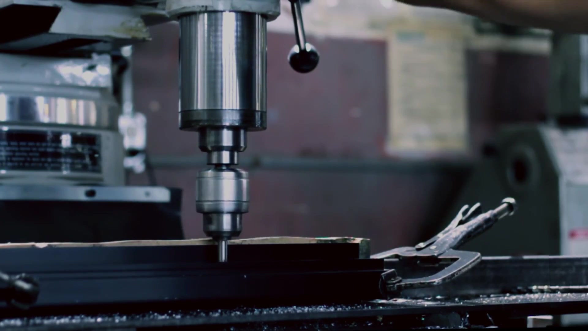
Manufaktur Custom Parts, Komponen, Rakitan, Produk Rampung, Mesin lan Peralatan Industri
Manufaktur Kontrak Domestik & Global
Outsourcing Produksi
Domestik, Pengadaan Global Produk Industri
Labeling pribadi / Label Putih Produk sampeyan nganggo Jeneng merek sampeyan
Product Finding & Locating Services
Desain Global lan Kemitraan Saluran
Integrasi Teknik
Layanan Teknik
Konsolidasi Global, Gudang, Logistik


Search Results
Looks like there's a technical issue. Clear your cookies and try again. If it still doesn't work, please contact us.