

Глобален прилагоден производител, интегратор, консолидатор, партнер за аутсорсинг за широк спектар на производи и услуги.
Ние сме ваш единствен извор за производство, изработка, инженерство, консолидација, интеграција, аутсорсинг на нарачано произведени и производи и услуги кои не се на полица. Ние, исто така, приватна етикета / бела етикета на вашите производи со името на вашиот бренд ако сакате.
Изберете го вашиот јазик
Прилагодено производство на делови, компоненти, склопови, готови производи, машини и индустриска опрема
Домашно и глобално договорно производство
Производство Аутсорсинг
Домашни, глобални набавки на индустриски производи
Приватно означување / Бело означување на вашите производи со вашето име на бренд
Услуги за пронаоѓање и лоцирање производи
Глобален дизајн и партнерство за канали
Инженерска интеграција
Инженерски услуги
Глобална консолидација, складирање, логистика


Search Results
164 results found with an empty search
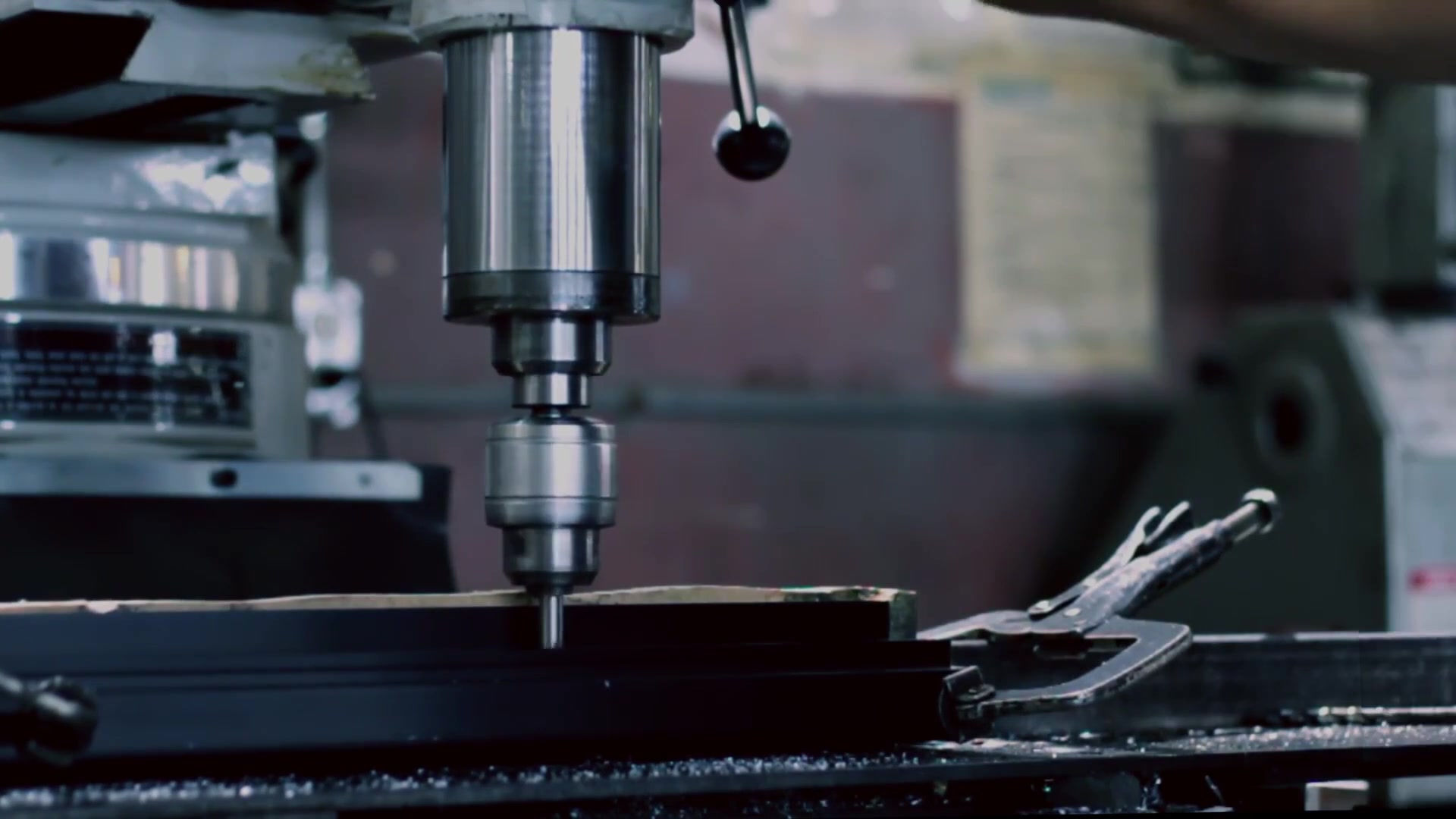
- Electrochemical Machining and Grinding - ECM - Reverse Electroplating
Electrochemical Machining and Grinding - ECM - Reverse Electroplating - Custom Machining - AGS-TECH Inc. - NM - USA ECM обработка, електрохемиска обработка, мелење Some of the valuable NON-CONVENTIONAL MANUFACTURING processes AGS-TECH Inc offers are ELECTROCHEMICAL MACHINING (ECM), SHAPED-TUBE ELECTROLYTIC MACHINING (STEM), PULSED ELECTROCHEMICAL MACHINING (PECM), ELECTROCHEMICAL GRINDING (ECG), HYBRID MACHINING PROCESSES. ELECTROCHEMICAL MACHINING (ECM) is a non-conventional manufacturing technique where metal is removed by an electrochemical process. ECM is typically a mass production technique, used for machining extremely hard materials and materials that are difficult to machine using the conventional manufacturing methods. Electrochemical-machining systems we use for production are numerically controlled machining centers with high production rates, flexibility, perfect control of dimensional tolerances. Electrochemical machining is capable of cutting small and odd-shaped angles, intricate contours or cavities in hard and exotic metals like titanium aluminides, Inconel, Waspaloy, and high nickel, cobalt, and rhenium alloys. Both external and internal geometries can be machined. Modifications of the electrochemical machining process are used for operations like turning, facing, slotting, trepanning, profiling where the electrode becomes the cutting tool. The metal removal rate is only a function of ion exchange rate and is not affected by the strength, hardness or toughness of the workpiece. Unfortunately the method of electrochemical machining (ECM) is limited to electrically conductive materials. Another important point to consider deploying the ECM technique is to compare the mechanical properties of the produced parts with those produced by other machining methods. ECM removes material instead of adding it and therefore is sometimes referred to as ''reverse electroplating''. It resembles in some ways to electrical discharge machining (EDM) in that a high current is passed between an electrode and the part, through an electrolytic material removal process having a negatively charged electrode (cathode), a conductive fluid (electrolyte), and a conductive workpiece (anode). The electrolyte acts as the current carrier and is a highly conductive inorganic salt solution like sodium chloride mixed and dissolved in water or sodium nitrate. The advantage of ECM is that there is no tool wear. The ECM cutting tool is guided along the desired path close to the work but without touching the piece. Unlike EDM, however, no sparks are created. High metal removal rates and mirror surface finishes are possible with ECM, with no thermal or mechanical stresses being transferred to the part. ECM does not cause any thermal damage to the part and since there are no tool forces there is no distortion to the part and no tool wear, as would be the case with typical machining operations. In electrochemical machining cavity produced is the female mating image of the tool. In the ECM process, a cathode tool is moved into an anode workpiece. The shaped tool is generally made of copper, brass, bronze or stainless steel. The pressurized electrolyte is pumped at a high rate at a set temperature through the passages in the tool to the area being cut. The feed rate is the same as the rate of ''liquification'' of the material, and the electrolyte movement in the tool-workpiece gap washes metal ions away from the workpiece anode before they have a chance to plate onto the cathode tool. The gap between the tool and the workpiece varies between 80-800 micrometers and the DC power supply in the range 5 – 25 V maintains current densities between 1.5 – 8 A/mm2 of active machined surface. As electrons cross the gap, material from the workpiece is dissolved, as the tool forms the desired shape in the workpiece. The electrolytic fluid carries away the metal hydroxide formed during this process. Commercial electrochemical machines with current capacities between 5A and 40,000A are available. The material removal rate in electrochemical machining can be expressed as: MRR = C x I x n Here MRR=mm3/min, I=current in amperes, n=current efficiency, C=a material constant in mm3/A-min. The constant C depends on valence for pure materials. The higher the valence, the lower is its value. For most metals it is in between 1 and 2. If Ao denotes the uniform cross-sectional area being electrochemically machined in mm2, the feed rate f in mm/min can be expressed as: F = MRR / Ao Feed rate f is the speed the electrode is penetrating the workpiece. In the past there were problems of poor dimensional accuracy and environmentally polluting waste from electrochemical machining operations. These have largely been overcome. Some of the applications of electrochemical machining of high-strength materials are: - Die-Sinking operations. Die-sinking is machining forging – die cavities. - Drilling a jet engine turbine blades, jet-engine parts and nozzles. - Multiple small holes drilling. The electrochemical machining process leaves a burr-free surface. - Steam turbine blades can be machined within close limits. - For deburring of surfaces. In deburring, ECM removes metal projections left from the machining processes and so dulls sharp edges. Electrochemical machining process is fast and often more convenient than the conventional methods of deburring by hand or non-traditional machining processes. SHAPED-TUBE ELECTROLYTIC MACHINING (STEM) is a version of electrochemical machining process we use for drilling small diameter deep holes. A titanium tube is used as the tool which is coated with an electrically insulating resin to prevent the removal of material from other regions like the lateral faces of the hole and tube. We can drill hole sizes of 0.5 mm with depth-to-diameter ratios of 300:1 PULSED ELECTROCHEMICAL MACHINING (PECM): We use very high pulsed current densities in the order of 100 A/cm2. By using pulsed currents we eliminate the need for high electrolyte flow rates which poses limitations for the ECM method in mold and die fabrication. Pulsed electrochemical machining improves fatigue life and eliminates the recast layer left by the electrical discharge machining (EDM) technique on mold and die surfaces. In ELECTROCHEMICAL GRINDING (ECG) we combine the conventional grinding operation with electrochemical machining. The grinding wheel is a rotating cathode with abrasive particles of diamond or aluminum oxide that are metal bonded. The current densities range between 1 and 3 A/mm2. Similar to ECM, an electrolyte such as sodium nitrate flows and the metal removal in electrochemical grinding is dominated by the electrolytic action. Less than 5% of metal removal is by abrasive action of the wheel. The ECG technique is well suited for carbides and high-strength alloys, but not so much of a fit for die-sinking or mould making because the grinder may not easily access deep cavities. The material removal rate in electrochemical grinding can be expressed as: MRR = G I / d F Here MRR is in mm3/min, G is mass in grams, I is current in amperes, d is density in g/mm3 and F is Faraday’s constant (96,485 Coulombs/mole). The speed of penetration of the grinding wheel into workpiece can be expressed as: Vs = (G / d F) x (E / g Kp) x K Here Vs is in mm3/min, E is cell voltage in volts, g is wheel to workpiece gap in mm, Kp is coefficient of loss and K is electrolyte conductivity. The advantage of the electrochemical grinding method over conventional grinding is less wheel wear because less than 5% of the metal removal is by abrasive action of the wheel. There are similarities between EDM and ECM: 1. The tool and workpiece are separated by a very small gap without a contact in between them. 2. Both tool and material must be conductors of electricity. 3. Both techniques need high capital investment. Modern CNC machines are used 4. Both methods consume lots of electric power. 5. A conductive fluid is used as a medium between the tool and the work piece for ECM and a dielectric fluid for EDM. 6. The tool is fed continuously towards the workpiece to maintain a constant gap between them (EDM may incorporate intermittent or cyclic, typically partial, tool withdrawal). HYBRID MACHINING PROCESSES: We frequently take advantage of the benefits of hybrid machining processes where two or more different processes such as ECM, EDM….etc. are used in combination. This gives us the opportunity to overcome the shortcomings of one process by the other, and benefit from the advantages of each process. КЛИКНЕТЕ Услуга за пронаоѓање на производи-локатор ПРЕТХОДНА СТРАНИЦА
- Passive Optical Components, Splitter & Combiner, DWDM, Optical Switch
Passive Optical Components - Splitter - Combiner - DWDM - Optical Switch - MUX / DEMUX - Circulator - Waveguide - EDFA Производство и склопување на пасивни оптички компоненти We supply PASSIVE OPTICAL COMPONENTS ASSEMBLY, including: • FIBER OPTICAL COMMUNICATION DEVICES: Fiberoptic taps, splitters-combiners, fixed and variable optical attenuators, optical switch, DWDM, MUX/DEMUX, EDFA, Raman amplifiers and other amplifiers, circulators, gain flatteners, custom fiber optic assemblies for telecommunication systems, optical waveguide devices, splicing enclosure, CATV products. • INDUSTRIAL FIBER OPTICAL ASSEMBLY: Fiber optic assemblies for industrial applications (illumination, light delivery or inspection of pipe interiors, fiberscopes, endoscopes....). • FREE SPACE PASSIVE OPTICAL COMPONENTS and ASSEMBLY: These are optical components made from special grade glasses and crystals with superior transmission and reflection and other outstanding characteristics. Lenses, prisms, beamsplitters, waveplates, polarizers, mirrors, filters......etc. are among this category. You can download our off-shelf passive free space optical components and assemblies from our catalog below or ask us for custom designing and manufacturing them specially for your application. Among the passive optical assemblies our engineers have developed are: - A test and cutting station for polarized attenuators. - Video endoscopes and fiberscopes for medical applications. We use special bonding and attachment techniques and materials for rigid, reliable and long life assemblies. Even under extensive environmental cycling tests such as high temperature/low temperature; high humidity/low humidity our assemblies remain intact and keep working. Passive optical components and assemblies have become commodities in recent years. There really is no need to pay big amounts for these components. Contact us to take advantage of our competitive prices for the highest quality available. All our passive optical components and assemblies are manufactured in ISO9001 and TS16949 certified plants and conform to relevant international standards such as Telcordia for communication optics and UL, CE for industrial optical assemblies. Passive Fiber Optic Components and Assembly Brochure Passive Free Space Optical Components and Assembly Brochure КЛИКНЕТЕ Услуга за пронаоѓање на производи-локатор ПРЕТХОДНА СТРАНИЦА
- Brushes, Brush Manufacturing, USA, AGS-TECH
AGS-TECH Inc. supplies off-the-shelf as well as custom manufactured brushes. Many types are offered including industrial brush, agricultural brushes, municipal brushes, copper wire brush, zig zag brush, roller brush, side brushes, metal polishing brush, window cleaning brushes, heavy industrial scrubbing brush...etc. Четки и четки Производство AGS-TECH has experts in the consultancy, design and manufacturing of brushes for cleaning and processing equipment manufacturers. We work with you to offer innovative custom brush design solutions. Brush prototypes are developed before volume production runs. We help you to design, develop and manufacture high quality brushes for optimal machine performance. Products can be produced almost at any dimensional specifications you prefer or is suitable for your application. Also the brush bristles can be of various lengths and materials. Both natural and synthetic bristles and materials are being used in our brushes depending on the application. Sometimes we are able to offer you an off-the-shelf brush that will fit your application and needs. Just let us know your needs and we are here to help you. Some of the types of brushes we are able to supply you are: Industrial Brushes Agricultural Brushes Vegetable Brushes Municipal Brushes Copper Wire Brush Zig Zag Brushes Roller Brush Side Brushes Roller Brushes Disk Brushes Circular Brushes Ring Brushes and Spacers Cleaning Brushes Conveyor Cleaning Brush Polishing Brushes Metal Polishing Brush Window Cleaning Brushes Glass Manufacturing Brushes Trommel Screen Brushes Strip Brushes Industrial Cylinder Brushes Brushes with Varying Bristle Lengths Variable & Adjustable Bristle Length Brushes Synthetic Fibers Brush Natural Fibers Brush Lath Brush Heavy Industrial Scrubbing Brushes Specialist Commercial Brushes If you do have detailed blueprints of brushes you need manufactured, that is perfect. Just send them to us for evaluation. If you do not have blueprints, no problem. A sample, a photo or a hand sketch of the brush may be sufficient initially for most projects. We will send you special templates to fill in your requirements and details so we can evaluate, design and manufacture your product correctly. In our templates we have questions on details such as: Brush face length Tube length Tube inside and outside diameters Disk inside and outside diameters Disk thickness Brush diameter Brush height Tuft diameter Density Material and color of bristles Bristle diameter Brush pattern & fill pattern (double row helical, double row chevron, full fill,….etc.) Brush drive of choice Applications for the brushes (food, pharmaceuticals, polishing of metals, industrial cleaning…etc.) With your brushes we can supply you accessories such as pad holders, hooked pads, necessary attachments, disk drives, drive coupling…etc. If you are unfamiliar with these brush specs, again no problem. We will guide you throughout the design process. PREVIOUS PAGE
- Micro-Optics - Micro-Optical - Microoptical - Wafer Level Optics
Micro-Optics, Micro-Optical, Microoptical, Wafer Level Optics, Gratings, Fresnel Lenses, Lens Array, Micromirrors, Micro Reflectors, Collimators, Aspheres, LED Производство на микро-оптика One of the fields in microfabrication we are involved in is MICRO-OPTICS MANUFACTURING. Micro-optics allows the manipulation of light and the management of photons with micron and sub-micron scale structures and components. Some applications of MICRO-OPTICAL COMPONENTS and SUBSYSTEMS are: Information technology: In micro-displays, micro-projectors, optical data storage, micro-cameras, scanners, printers, copiers…etc. Biomedicine: Minimally-invasive/point of care diagnostics, treatment monitoring, micro-imaging sensors, retinal implants, micro-endoscopes. Lighting: Systems based on LEDs and other efficient light sources Safety and Security Systems: Infrared night vision systems for automotive applications, optical fingerprint sensors, retinal scanners. Optical Communication & Telecommunication: In photonic switches, passive fiber optic components, optical amplifiers, mainframe and personal computer interconnect systems Smart structures: In optical fiber-based sensing systems and much more The types of micro-optical components and subsystems we manufacture and supply are: - Wafer Level Optics - Refractive Optics - Diffractive Optics - Filters - Gratings - Computer Generated Holograms - Hybrid Microoptical Components - Infrared Micro-Optics - Polymer Micro-Optics - Optical MEMS - Monolithically and Discretely Integrated Micro-Optic Systems Some of our most widely used micro-optical products are: - Bi-convex and plano-convex lenses - Achromat lenses - Ball lenses - Vortex Lenses - Fresnel Lenses - Multifocal Lens - Cylindrical Lenses - Graded Index (GRIN) Lenses - Micro-Optical Prisms - Aspheres - Arrays of Aspheres - Collimators - Micro-Lens Arrays - Diffraction Gratings - Wire-Grid Polarizers - Micro-Optic Digital Filters - Pulse Compression Gratings - LED Modules - Beam Shapers - Beam Sampler - Ring Generator - Micro-Optical Homogenizers / Diffusers - Multispot Beam Splitters - Dual Wavelength Beam Combiners - Micro-Optical Interconnects - Intelligent Micro-Optics Systems - Imaging Microlenses - Micromirrors - Micro Reflectors - Micro-Optical Windows - Dielectric Mask - Iris Diaphragms Let us provide you some basic information about these micro-optical products and their applications: BALL LENSES: Ball lenses are completely spherical micro-optic lenses most commonly used to couple light in and out of fibers. We supply a range of micro-optic stock ball lenses and can manufacture also to your own specifications. Our stock ball lenses from quartz have excellent UV and IR transmission between 185nm to >2000nm, and our sapphire lenses have a higher refractive index, allowing a very short focal length for excellent fiber coupling. Micro-optical ball lenses from other materials and diameters are available. Besides fiber coupling applications, micro-optical ball lenses are used as objective lenses in endoscopy, laser measurement systems and bar-code scanning. On the other hand, micro-optic half ball lenses offer uniform dispersion of light and are widely used in LED displays and traffic lights. MICRO-OPTICAL ASPHERES and ARRAYS: Aspheric surfaces have a non-spherical profile. Use of aspheres can reduce the number of optics required to reach a desired optical performance. Popular applications for micro-optical lens arrays with spherical or aspherical curvature are imaging and illumination and the effective collimation of laser light. Substitution of a single aspheric microlens array for a complex multilens system results not only in smaller size, lighter weight, compact geometry, and lower cost of an optical system, but also in significant improvement of its optical performance such as better imaging quality. However, the fabrication of aspheric microlenses and microlens arrays is challenging, because conventional technologies used for macro-sized aspheres like single-point diamond milling and thermal reflow are not capable of defining a complicated micro-optic lens profile in an area as small as several to tens of micrometers. We possess the know-how of producing such micro-optical structures using advanced techniques such as femtosecond lasers. MICRO-OPTICAL ACHROMAT LENSES: These lenses are ideal for applications requiring color correction, while aspheric lenses are designed to correct spherical aberration. An achromatic lens or achromat is a lens that is designed to limit the effects of chromatic and spherical aberration. Micro-optical achromatic lenses make corrections to bring two wavelengths (such as red and blue colors) into focus on the same plane. CYLINDRICAL LENSES: These lenses focus light into a line instead of a point, as a spherical lens would. The curved face or faces of a cylindrical lens are sections of a cylinder, and focus the image passing through it into a line parallel to the intersection of the surface of the lens and a plane tangent to it. The cylindrical lens compresses the image in the direction perpendicular to this line, and leaves it unaltered in the direction parallel to it (in the tangent plane). Tiny micro-optical versions are available which are suitable for use in micro optical environments, requiring compact-size fiber optical components, laser systems, and micro-optical devices. MICRO-OPTICAL WINDOWS and FLATS: Milimetric micro-optical windows meeting tight tolerance requirements are available. We can custom manufacture them to your specifications from any of the optical grade glasses. We offer a variety of micro-optical windows made of different materials such as fused silica, BK7, sapphire, zinc sulphide….etc. with transmission from UV to middle IR range. IMAGING MICROLENSES: Microlenses are small lenses, generally with a diameter less than a millimetre (mm) and as small as 10 micrometres. Imaging Lenses are used to view objects in imaging systems. Imaging Lenses are used in imaging systems to focus an image of an examined object onto a camera sensor. Depending on the lens, imaging lenses can be used to remove parallax or perspective error. They can also offer adjustable magnifications, field of views, and focal lengths. These lenses allow an object to be viewed in several ways to illustrate certain features or characteristics that may be desirable in certain applications. MICROMIRRORS: Micromirror devices are based on microscopically small mirrors. The mirrors are Microelectromechanical systems (MEMS). The states of these micro-optical devices are controlled by applying a voltage between the two electrodes around the mirror arrays. Digital micromirror devices are used in video projectors and optics and micromirror devices are used for light deflection and control. MICRO-OPTIC COLLIMATORS & COLLIMATOR ARRAYS: A variety of micro-optical collimators are available off-the-shelf. Micro-optical small beam collimators for demanding applications are produced using laser fusion technology. The fiber end is directly fused to the optical center of the lens, thereby eliminated epoxy within the optical path. The micro-optic collimator lens surface is then laser polished to within a millionth of an inch of the ideal shape. Small Beam collimators produce collimated beams with beam waists under a millimeter. Micro-optical small beam collimators are typically used at 1064, 1310 or 1550 nm wavelengths. GRIN lens based micro-optic collimators are also available as well as collimator array and collimator fiber array assemblies. MICRO-OPTICAL FRESNEL LENSES: A Fresnel lens is a type of compact lens designed to allow the construction of lenses of large aperture and short focal length without the mass and volume of material that would be required by a lens of conventional design. A Fresnel lens can be made much thinner than a comparable conventional lens, sometimes taking the form of a flat sheet. A Fresnel lens can capture more oblique light from a light source, thus allowing the light to be visible over greater distances. The Fresnel lens reduces the amount of material required compared to a conventional lens by dividing the lens into a set of concentric annular sections. In each section, the overall thickness is decreased compared to an equivalent simple lens. This can be viewed as dividing the continuous surface of a standard lens into a set of surfaces of the same curvature, with stepwise discontinuities between them. Micro-optic Fresnel lenses focus light by refraction in a set of concentric curved surfaces. These lenses can be made very thin and lightweight. Micro-optical Fresnel lenses offer opportunities in optics for highresolution Xray applications, throughwafer optical interconnection capabilities. We have a number of fabrication methods including micromolding and micromachining to manufacture micro-optical Fresnel lenses and arrays specifically for your applications. We can design a positive Fresnel lens as a collimator, collector or with two finite conjugates. Micro-Optical Fresnel lenses are usually corrected for spherical aberrations. Micro-optic positive lenses can be metalized for use as a second surface reflector and negative lenses can be metalized for use as a first surface reflector. MICRO-OPTICAL PRISMS: Our line of precision micro-optics includes standard coated and uncoated micro prisms. They are suitable for use with laser sources and imaging applications. Our micro-optical prisms have submilimeter dimensions. Our coated micro-optical prisms can also be used as mirror reflectors with respect to incoming light. Uncoated prisms act as mirrors for light incident on one of the short sides since incident light is totally internally reflected at the hypotenuse. Examples of our micro-optical prism capabilities include right angle prisms, beamsplitter cube assemblies, Amici prisms, K-prisms, Dove prisms, Roof prisms, Cornercubes, Pentaprisms, Rhomboid prisms, Bauernfeind prisms, Dispersing prisms, Reflecting prisms. We also offer light guiding and de-glaring optical micro-prisms made from acrylic, polycarbonate and other plastic materials by hot embossing manufacturing process for applications in lamps and luminaries, LEDs. They are highly efficient, strong light guiding precise prism surfaces, support luminaries to fulfill office regulations for de-glaring. Additional customized prism structures are possible. Microprisms and microprism arrays on wafer level are also possible using microfabrication techniques. DIFFRACTION GRATINGS: We offer design and manufacture of diffractive micro-optical elements (DOEs). A diffraction grating is an optical component with a periodic structure, which splits and diffracts light into several beams travelling in different directions. The directions of these beams depend on the spacing of the grating and the wavelength of the light so that the grating acts as the dispersive element. This makes grating a suitable element to be used in monochromators and spectrometers. Using wafer-based lithography, we produce diffractive micro-optical elements with exceptional thermal, mechanical and optical performance characteristics. Wafer-level processing of micro-optics provides excellent manufacturing repeatability and economic output. Some of the available materials for diffractive micro-optical elements are crystal-quartz, fused-silica, glass, silicon and synthetic substrates. Diffraction gratings are useful in applications such as spectral analysis / spectroscopy, MUX/DEMUX/DWDM, precision motion control such as in optical encoders. Lithography techniques make the fabrication of precision micro-optical gratings with tightly-controlled groove spacings possible. AGS-TECH offers both custom and stock designs. VORTEX LENSES: In laser applications there is a need to convert a Gaussian beam to a donut-shaped energy ring. This is achieved using Vortex lenses. Some applications are in lithography and high-resolution microscopy. Polymer on glass Vortex phase plates are also available. MICRO-OPTICAL HOMOGENIZERS / DIFFUSERS: A variety of technologies are used to fabricate our micro-optical homogenizers and diffusers, including embossing, engineered diffuser films, etched diffusers, HiLAM diffusers. Laser Speckle is the optical phenomena resulting from the random interference of coherent light. This phenomenon is utilized to measure the Modulation Transfer Function (MTF) of detector arrays. Microlens diffusers are shown to be efficient micro-optic devices for speckle generation. BEAM SHAPERS: A micro-optic beam shaper is an optic or a set of optics that transforms both the intensity distribution and the spatial shape of a laser beam to something more desirable for a given application. Frequently, a Gaussian-like or non-uniform laser beam is transformed to a flat top beam. Beam shaper micro-optics are used to shape and manipulate single mode and multi-mode laser beams. Our beam shaper micro-optics provide circular, square, rectilinear, hexagonal or line shapes, and homogenize the beam (flat top) or provide a custom intensity pattern according to the requirements of the application. Refractive, diffractive and reflective micro-optical elements for laser beam shaping and homogenizing have been manufactured. Multifunctional micro-optical elements are used for shaping arbitrary laser beam profiles into a variety of geometries like, a homogeneous spot array or line pattern, a laser light sheet or flat-top intensity profiles. Fine beam application examples are cutting and keyhole welding. Broad beam application examples are conduction welding, brazing, soldering, heat treatment, thin film ablation, laser peening. PULSE COMPRESSION GRATINGS: Pulse compression is a useful technique that takes advantage of the relationship between pulse duration and spectral width of a pulse. This enables the amplification of laser pulses above the normal damage threshold limits imposed by the optical components in the laser system. There are linear and nonlinear techniques for reducing the durations of optical pulses. There is variety of methods for temporally compressing / shortening optical pulses, i.e., reducing the pulse duration. These methods generally start in the picosecond or femtosecond region, i.e. already in the regime of ultrashort pulses. MULTISPOT BEAM SPLITTERS: Beam splitting by means of diffractive elements is desirable when one element is required to produce several beams or when very exact optical power separation is required. Precise positioning can also be achieved, for example, to create holes at clearly defined and accurate distances. We have Multi-Spot Elements, Beam Sampler Elements, Multi-Focus Element. Using a diffractive element, collimated incident beams are split into several beams. These optical beams have equal intensity and equal angle to one another. We have both one-dimensional and two-dimensional elements. 1D elements split beams along a straight line whereas 2D elements produce beams arranged in a matrix of, for example, 2 x 2 or 3 x 3 spots and elements with spots that are arranged hexagonally. Micro-optical versions are available. BEAM SAMPLER ELEMENTS: These elements are gratings that are used for inline monitoring of high power lasers. The ± first diffraction order can be used for beam measurements. Their intensity is significantly lower than that of the main beam and can be custom designed. Higher diffraction orders can also be used for measurement with even lower intensity. Variations in intensity and changes in the beam profile of high power lasers can be reliably monitored inline using this method. MULTI-FOCUS ELEMENTS: With this diffractive element several focal points can be created along the optical axis. These optical elements are used in sensors, ophthalmology, material processing. Micro-optical versions are available. MICRO-OPTICAL INTERCONNECTS: Optical interconnects have been replacing electrical copper wires at the different levels in the interconnect hierarchy. One of the possibilities to bring the advantages of micro-optics telecommunications to the computer backplane, the printed circuit board, the inter-chip and on-chip interconnect level, is to use free-space micro-optical interconnect modules made of plastic. These modules are capable of carrying high aggregate communication bandwidth through thousands of point-to-point optical links on a footprint of a square centimeter. Contact us for off-shelf as well as custom tailored micro-optical interconnects for computer backplane, the printed circuit board, the inter-chip and on-chip interconnect levels. INTELLIGENT MICRO-OPTICS SYSTEMS: Intelligent micro-optic light modules are used in smart phones and smart devices for LED flash applications, in optical interconnects for transporting data in supercomputers and telecommunications equipment, as miniaturized solutions for near-infrared beam shaping, detection in gaming applications and for supporting gesture control in natural user interfaces. Sensing opto-electronic modules are used for a number of product applications such as ambient light and proximity sensors in smart phones. Intelligent imaging micro-optic systems are used for primary and front-facing cameras. We offer also customized intelligent micro-optical systems with high performance and manufacturability. LED MODULES: You can find our LED chips, dies and modules on our page Lighting & Illumination Components Manufacturing by clicking here. WIRE-GRID POLARIZERS: These consist of a regular array of fine parallel metallic wires, placed in a plane perpendicular to the incident beam. The polarization direction is perpendicular to the wires. Patterned polarizers have applications in polarimetry, interferometry, 3D displays, and optical data storage. Wire-grid polarizers are extensively used in infrared applications. On the other hand micropatterned wire-grid polarizers have limited spatial resolution and poor performance at visible wavelengths, are susceptible to defects and cannot be easily extended to non-linear polarizations. Pixelated polarizers use an array of micro-patterned nanowire grids. The pixelated micro-optical polarizers can be aligned with cameras, plane arrays, interferometers, and microbolometers without the need for mechanical polarizer switches. Vibrant images distinguishing between multiple polarizations across the visible and IR wavelengths can be captured simultaneously in real-time enabling fast, high resolution images. Pixelated micro-optical polarizers also enable clear 2D and 3D images even in low-light conditions. We offer patterned polarizers for two, three and four-state imaging devices. Micro-optical versions are available. GRADED INDEX (GRIN) LENSES: Gradual variation of the refractive index (n) of a material can be used to produce lenses with flat surfaces, or lenses that do not have the aberrations typically observed with traditional spherical lenses. Gradient-index (GRIN) lenses may have a refraction gradient that is spherical, axial, or radial. Very small micro-optical versions are available. MICRO-OPTIC DIGITAL FILTERS: Digital neutral density filters are used to control the intensity profiles of illumination and projection systems. These micro-optic filters contain well-defined metal absorber micro-structures that are randomly distributed on a fused silica substrate. Properties of these micro-optical components are high accuracy, large clear aperture, high damage threshold, broadband attenuation for DUV to IR wavelengths, well defined one or two dimensional transmission profiles. Some applications are soft edge apertures, precise correction of intensity profiles in illumination or projection systems, variable attenuation filters for high-power lamps and expanded laser beams. We can customize the density and size of the structures to meet precisely the transmission profiles required by the application. MULTI-WAVELENGTH BEAM COMBINERS: Multi-Wavelength beam combiners combine two LED collimators of different wavelengths into a single collimated beam. Multiple combiners can be cascaded to combine more than two LED collimator sources. Beam combiners are made of high-performance dichroic beam splitters that combine two wavelengths with >95% efficiency. Very small micro-optic versions are available. КЛИКНЕТЕ Услуга за пронаоѓање на производи-локатор ПРЕТХОДНА СТРАНИЦА
- Mesomanufacturing,Mesoscale Manufacturing,Miniature Device Fabrication
Mesomanufacturing - Mesoscale Manufacturing - Miniature Device Fabrication - Tiny Motors - AGS-TECH Inc. - New Mexico Мезоскала Производство / Мезопроизводство With conventional production techniques we produce “macroscale” structures that are relatively large and visible to the naked eye. With MESOMANUFACTURING however we produce components for miniature devices. Mesomanufacturing is also referred to as MESOSCALE MANUFACTURING or MESO-MACHINING. Mesomanufacturing overlaps both macro and micromanufacturing. Examples of mesomanufacturing are hearing aides, stents, very small motors. The first approach in mesomanufacturing is to scale macromanufacturing processes down. For example a tiny lathe with dimensions in the few dozen millimeters and a motor of 1.5W weighing 100 grams is a good example of mesomanufacturing where downscaling has taken place. The second approach is to scale micromanufacturing processes up. As an example LIGA processes can be upscaled and enter the realm of mesomanufacturing. Our mesomanufacturing processes are bridging the gap between silicon-based MEMS processes and conventional miniature machining. Mesoscale processes can fabricate two and three-dimensional parts having micron size features in traditional materials such as stainless steels, ceramics, and glass. Mesomanufacturing processes that are currently available to us include, focused ion beam (FIB) sputtering, micro-milling, micro-turning, excimer laser ablation, femto-second laser ablation, and micro electro-discharge (EDM) machining. These mesoscale processes employ subtractive machining technologies (i.e., material removal), whereas the LIGA process, is an additive mesoscale process. Mesomanufacturing processes have different capabilities and performance specifications. Machining performance specifications of interest include minimum feature size, feature tolerance, feature location accuracy, surface finish, and material removal rate (MRR). We have the capability of mesomanufacturing electro-mechanical components that require mesoscale parts. The mesoscale parts fabricated by subtractive mesomanufacturing processes have unique tribological properties because of the variety of materials and the surface conditions produced by the different mesomanufacturing processes. These subtractive mesoscale machining technologies bring us concerns related to cleanliness, assembly, and tribology. Cleanliness is vital in mesomanufacturing because mesoscale dirt and debris particle size created during the meso-machining process can be comparable to mesoscale features. Mesoscale milling and turning can create chips and burrs that can block holes. Surface morphology and surface finish conditions vary greatly depending on the mesomanufacturing method. Mesoscale parts are difficult to handle and align which makes assembly a challenge which most of our competitors are unable to overcome. Our yield rates in mesomanufacturing is far higher than our competitors which gives us the advantage of being able to offer better prices. MESOSCALE MACHINING PROCESSES: Our major mesomanufacturing techniques are Focused Ion Beam (FIB), Micro-milling, & Micro-turning, laser meso-machining, Micro-EDM (electro-discharge machining) Mesomanufacturing using focused Ion Beam (FIB), Micro-milling, & Micro-turning: The FIB sputters material from a workpiece by Gallium ion beam bombardment. The workpiece is mounted to a set of precision stages and is placed in a vacuum chamber underneath the source of Gallium. The translation and rotation stages in the vacuum chamber make various locations on the work piece available to the beam of Gallium ions for FIB mesomanufacturing. A tunable electric field scans the beam to cover a pre-defined projected area. A high voltage potential causes a source of Gallium ions to accelerate and collide with the work piece. The collisions strip away atoms from the work piece. The result of the FIB meso-machining process can be the creation of a near vertical facets. Some FIBs available to us have beam diameters as small as 5 nanometers, making the FIB a mesoscale and even microscale capable machine. We mount micro-milling tools on high precision milling machines to machine channels in aluminum. Using FIB we can fabricate micro-turning tools which can then be used on a lathe to fabricate finely threaded rods. In other words, FIB can be used to machine hard tooling besides directly meso-machining features onto the end work piece. The slow material removal rate has rendered the FIB as impractical for directly machining large features. The hard tools, however, can remove material at an impressive rate and are durable enough for several hours of machining time. Nevertheless, the FIB is practical for directly meso-machining complex three dimensional shapes that do not require a substantial material removal rate. Length of exposure and angle of incidence can greatly affect the geometry of directly machined features. Laser Mesomanufacturing: Excimer lasers are used for mesomanufacturing. The excimer laser machines material by pulsing it with nanosecond pulses of ultraviolet light. The work piece is mounted to precision translational stages. A controller coordinates the motion of the work piece relative to the stationary UV laser beam and coordinates the firing of the pulses. A mask projection technique can be used to define meso-machining geometries. The mask is inserted into the expanded part of the beam where the laser fluence is too low to ablate the mask. The mask geometry is de-magnified through the lens and projected onto the work piece. This approach can be used for machining multiple holes (arrays) simultaneously. Our excimer and YAG lasers can be used to machine polymers, ceramics, glass and metals having feature sizes as small as 12 microns. Good coupling between the UV wavelength (248 nm) and the workpiece in laser mesomanufacturing / meso-machining results in vertical channel walls. A cleaner laser meso-machining approach is to use a Ti-sapphire femtosecond laser. The detectable debris from such mesomanufacturing processes are nano-sized particles. Deep one micron-size features can be microfabricated using the femtosecond laser. The femtosecond laser ablation process is unique in that it breaks atomic bonds instead of thermally ablating material. The femtosecond laser meso-machining / micromachining process has a special place in mesomanufacturing because it is cleaner, micron capable, and it is not material specific. Mesomanufacturing using Micro-EDM (electro-discharge machining): Electro-discharge machining removes material through a spark erosion process. Our micro-EDM machines can produce features as small as 25 microns. For the sinker and the wire micro-EDM machine, the two major considerations for determining feature size are the electrode size and the over-bum gap. Electrodes little over 10 microns in diameter and over-bum as little as a few microns are being used. Creating an electrode having a complex geometry for the sinker EDM machine requires know-how. Both graphite and copper are popular as electrode materials. One approach to fabricating a complicated sinker EDM electrode for a mesoscale part is to use the LIGA process. Copper, as the electrode material, can be plated into LIGA molds. The copper LIGA electrode can then be mounted onto the sinker EDM machine for mesomanufacturing a part in a different material such as stainless steel or kovar. No one mesomanufacturing process is sufficient for all operations. Some mesoscale processes are more wide reaching than others, but each process has its niche. Most of the time we require a variety of materials to optimize performance of mechanical components and are comfortable with traditional materials such as stainless steel because these materials have a long history and have been very well characterized through the years. Mesomanufacturing processes allow us to use traditional materials. Subtractive mesoscale machining technologies expand our material base. Galling may be an-issue with some material combinations in mesomanufacturing. Each particular mesoscale machining process uniquely affects the surface roughness and morphology. Micro-milling and micro-turning may generate burrs and particles that can cause mechanical problems. Micro-EDM may leave a recast layer that can have particular wear and friction characteristics. Friction effects between mesoscale parts may have limited points of contact and are not accurately modeled by surface contact models. Some mesoscale machining technologies, such as micro-EDM, are fairly mature, as opposed to others, such as femtosecond laser meso-machining, which still require additional development. КЛИКНЕТЕ Услуга за пронаоѓање на производи-локатор ПРЕТХОДНА СТРАНИЦА
- Industrial Chemicals, Industrial Consumables, Aerosols, Sprays, Industrial Chemical Agents
Industrial Chemicals, Industrial Consumables, Aerosols, Sprays, Industrial Chemical Agents Индустриски хемикалии и потрошен материјал There are many specialty chemicals that are use in the industry. Contact us if you would like to know how we can help you formulating and producing a specialty chemical product. We also offer some off-the-shelf chemical products that are used in various industrial applications such as the automotive and motor vehicle industries, electronic industry, optical industry, medical facilities, clean rooms, pharmaceutical plants.....etc. Please note that we engineer, design and manufacture products to your needs and specifications. We can either manufacture products according to your specifications or, If desired, we can help you in choosing the right materials and designing the product. You can click on the blue highlighted text below and download the industrial chemicals and consumables product brochures: - Filters & Filtration Products & Membranes - Private Label Aerosols and Sprays We can label these products with your name and logo if you wish - Private Label Cleanroom Consumables and Apparel We can label these products with your name and logo if you wish - Private Label Epoxy Solutions for Construction, Electrical, Industrial Assembly (We can put your name, label, logo on these epoxies if you wish) - Private Label Nano Surface Protection Car Care Products We can label these products with your name and logo if you wish - Private Label Nano Surface Protection Industrial Products We can label these products with your name and logo if you wish - Private Label Nano Surface Protection Marine Products We can label these products with your name and logo if you wish - Private Label Nano Surface Protection Products We can label these products with your name and logo if you wish - Private Label Tapes for Every Application We can label these products with your name and logo if you wish ПРЕТХОДНА СТРАНИЦА
- Laser Machining, LM, Laser Cutting, CO2 Laser Processing, Nd-YAG Cut
Laser Machining - LM - Laser Cutting - Custom Parts Manufacturing - CO2 Laser Processing - Nd-YAG - Cutting - Boring Laser Machining & Cutting & LBM LASER CUTTING is a HIGH-ENERGY-BEAM MANUFACTURING technology that uses a laser to cut materials, and is typically used for industrial manufacturing applications. In LASER BEAM MACHINING (LBM), a laser source focuses optical energy on the surface of the workpiece. Laser cutting directs the highly focused and high-density output of a high-power laser, by computer, at the material to be cut. The targeted material then either melts, burns, vaporizes away, or is blown away by a jet of gas, in a controlled manner leaving an edge with a high-quality surface finish. Our industrial laser cutters are suitable for cutting flat-sheet material as well as structural and piping materials, metallic and nonmetallic workpieces. Generally no vacuum is required in the laser beam machining and cutting processes. There are several types of lasers used in laser cutting and manufacturing. The pulsed or continuous wave CO2 LASER is suited for cutting, boring, and engraving. The NEODYMIUM (Nd) and neodymium yttrium-aluminum-garnet (Nd-YAG) LASERS are identical in style and differ only in application. The neodymium Nd is used for boring and where high energy but low repetition is required. The Nd-YAG laser on the other hand is used where very high power is required and for boring and engraving. Both CO2 and Nd/ Nd-YAG lasers can be used for LASER WELDING. Other lasers we use in manufacturing include Nd:GLASS, RUBY and EXCIMER. In Laser Beam Machining (LBM), the following parameters are important: The reflectivity and thermal conductivity of the workpiece surface and its specific heat and latent heat of melting and evaporation. The efficiency of the Laser Beam Machining (LBM) process increases with decreasing of these parameters. The cutting depth can be expressed as: t ~ P / (v x d) This means, the cutting depth “t” is proportional to the power input P and inversely proportional to cutting speed v and laser-beam spot diameter d. The surface produced with LBM is generally rough and has a heat-affected zone. CARBONDIOXIDE (CO2) LASER CUTTING and MACHINING: The DC-excited CO2 lasers get pumped by passing a current through the gas mix whereas the RF-excited CO2 lasers use radio frequency energy for excitation. The RF method is relatively new and has become more popular. DC designs require electrodes inside the cavity, and therefore they can have electrode erosion and plating of electrode material on the optics. To the contrary, RF resonators have external electrodes and therefore they are not prone to those problems. We use CO2 lasers in industrial cutting of many materials such as mild steel, aluminum, stainless steel, titanium and plastics. YAG LASER CUTTING and MACHINING: We use YAG lasers for cutting and scribing metals and ceramics. The laser generator and external optics require cooling. Waste heat is generated and transferred by a coolant or directly to air. Water is a common coolant, usually circulated through a chiller or heat transfer system. EXCIMER LASER CUTTING and MACHINING: An excimer laser is a kind of laser with wavelengths in the ultraviolet region. The exact wavelength depends on the molecules used. For example the following wavelengths are associated with the molecules shown in parantheses: 193 nm (ArF), 248 nm (KrF), 308 nm (XeCl), 353 nm (XeF). Some excimer lasers are tunable. Excimer lasers have the attractive property that they can remove very fine layers of surface material with almost no heating or change to the remainder of the material. Therefore excimer lasers are well suited to precision micromachining of organic materials such as some polymers and plastics. GAS-ASSISTED LASER CUTTING: Sometimes we use laser beams in combination with a gas stream, like oxygen, nitrogen or argon for cutting thin sheet materials. This is done using a LASER-BEAM TORCH. For stainless steel and aluminum we use high-pressure inert-gas-assisted laser cutting using nitrogen. This results in oxide-free edges to improve weldability. These gas streams also blow away molten and vaporized material from workpiece surfaces. In a LASER MICROJET CUTTING we have a water-jet guided laser in which a pulsed laser beam is coupled into a low-pressure water jet. We use it to perform laser cutting while using the water jet to guide the laser beam, similar to an optical fiber. The advantages of laser microjet are that the water also removes debris and cools the material, it is faster than traditional ''dry'' laser cutting with higher dicing speeds, parallel kerf and omnidirectional cutting capability. We deploy different methods in cutting using lasers. Some of the methods are vaporization, melt and blow, melt blow and burn, thermal stress cracking, scribing, cold cutting and burning, stabilized laser cutting. - Vaporization cutting: The focused beam heats the surface of the material to its boiling point and creates a hole. The hole leads to a sudden increase in absorptivity and quickly deepens the hole. As the hole deepens and the material boils, the generated vapor erodes the molten walls blowing material out and further enlarging the hole. Non melting material such as wood, carbon and thermoset plastics are usually cut by this method. - Melt and blow cutting: We use high-pressure gas to blow molten material from the cutting area, decreasing the required power. The material is heated to its melting point and then a gas jet blows the molten material out of the kerf. This eliminates the need to raise the temperature of the material any further. We cut metals with this technique. - Thermal stress cracking: Brittle materials are sensitive to thermal fracture. A beam is focused on the surface causing localized heating and thermal expansion. This results in a crack that can then be guided by moving the beam. We use this technique in glass cutting. - Stealth dicing of silicon wafers: The separation of microelectronic chips from silicon wafers is performed by the stealth dicing process, using a pulsed Nd:YAG laser, the wavelength of 1064 nm is well adopted to the electronic band gap of silicon (1.11 eV or 1117 nm). This is popular in semiconductor device fabrication. - Reactive cutting: Also called flame cutting, this technique can be resembled to oxygen torch cutting but with a laser beam as the ignition source. We use this for cutting carbon steel in thicknesses over 1 mm and even very thick steel plates with little laser power. PULSED LASERS provide us a high-power burst of energy for a short period and are very effective in some laser cutting processes, such as piercing, or when very small holes or very low cutting speeds are required. If a constant laser beam was used instead, the heat could reach the point of melting the entire piece being machined. Our lasers have the ability to pulse or cut CW (Continuous Wave) under NC (numerical control) program control. We use DOUBLE PULSE LASERS emitting a series of pulse pairs to improve material removal rate and hole quality. The first pulse removes material from the surface and the second pulse prevents the ejected material from readhering to the side of the hole or cut. Tolerances and surface finish in laser cutting and machining are outstanding. Our modern laser cutters have positioning accuracies in the neighborhood of 10 micrometers and repeatabilities of 5 micrometers. Standard roughnesses Rz increase with the sheet thickness, but decreases with laser power and cutting speed. The laser cutting and machining processes are capable of achieving close tolerances, often to within 0.001 inch (0.025 mm) Part geometry and the mechanical features of our machines are optimized to achieve best tolerance capabilities. Surface finishes we can obtain from laser beam cutting may range between 0.003 mm to 0.006 mm. Generally we easily achieve holes with 0.025 mm diameter, and holes as small as 0.005 mm and hole depth-to-diameter ratios of 50 to 1 have been produced in various materials. Our simplest and most standard laser cutters will cut carbon steel metal from 0.020–0.5 inch (0.51–13 mm) in thickness and can easily be up to thirty times faster than standard sawing. Laser-beam machining is used widely for drilling and cutting of metals, nonmetals and composite materials. Advantages of laser cutting over mechanical cutting include easier workholding, cleanliness and reduced contamination of the workpiece (since there is no cutting edge as in traditional milling or turning which can become contaminated by the material or contaminate the material, i.e. bue build-up). The abrasive nature of composite materials may make them difficult to machine by conventional methods but easy by laser machining. Because the laser beam does not wear during the process, precision obtained may be better. Because laser systems have a small heat-affected zone, there is also a lesser chance of warping the material that is being cut. For some materials laser cutting can be the only option. Laser-beam cutting processes are flexible, and fiber optic beam delivery, simple fixturing, short set-up times, availability of three dimensional CNC systems make it possible for laser cutting and machining to compete successfully with other sheet metal fabrication processes such as punching. This being said, laser technology can sometimes be combined with the mechanical fabrication technologies for improved overall efficiency. Laser cutting of sheet metals has the advantages over plasma cutting of being more precise and using less energy, however, most industrial lasers cannot cut through the greater metal thickness that plasma can. Lasers operating at higher powers such as 6000 Watts are approaching plasma machines in their ability to cut through thick materials. However the capital cost of these 6000 Watt laser cutters is much higher than that of plasma cutting machines capable of cutting thick materials like steel plate. There are also disadvantages of laser cutting and machining. Laser cutting involves high power consumption. Industrial laser efficiencies may range from 5% to 15%. The power consumption and efficiency of any particular laser will vary depending on output power and operating parameters. This will depend on type of laser and how well the laser matches the work at hand. Amount of laser cutting power required for a particular task depends on the material type, thickness, process (reactive/inert) used and the desired cutting rate. The maximum production rate in laser cutting and machining is limited by a number of factors including laser power, process type (whether reactive or inert), material properties and thickness. In LASER ABLATION we remove material from a solid surface by irradiating it with a laser beam. At low laser flux, the material is heated by the absorbed laser energy and evaporates or sublimates. At high laser flux, the material is typically converted to a plasma. High power lasers clean a large spot with a single pulse. Lower power lasers use many small pulses which may be scanned across an area. In laser ablation we remove material with a pulsed laser or with a continuous wave laser beam if the laser intensity is high enough. Pulsed lasers can drill extremely small, deep holes through very hard materials. Very short laser pulses remove material so quickly that the surrounding material absorbs very little heat, therefore laser drilling can be done on delicate or heat-sensitive materials. Laser energy can be selectively absorbed by coatings, therefore CO2 and Nd:YAG pulsed lasers can be used to clean surfaces, remove paint and coating, or prepare surfaces for painting without damaging the underlying surface. We use LASER ENGRAVING and LASER MARKING to engrave or mark an object. These two techniques are in fact the most widely used applications. No inks are used, nor does it involve tool bits which contact the engraved surface and wear out which is the case with traditional mechanical engraving and marking methods. Materials specially designed for laser engraving and marking include laser-sensitive polymers and special new metal alloys. Although laser marking and engraving equipment is relatively more expensive compared to alternatives such as punches, pins, styli, etching stamps….etc., they have become more popular due to their accuracy, reproducibility, flexibility, ease of automation and on-line application in a wide variety of manufacturing environments. Finally, we use laser beams for several other manufacturing operations: - LASER WELDING - LASER HEAT TREATING: Small-scale heat treating of metals and ceramics to modify their surface mechanical and tribological properties. - LASER SURFACE TREATMENT / MODIFICATION: Lasers are used to clean surfaces, introduce functional groups, modify surfaces in an effort to improve adhesion prior to coating deposition or joining processes. КЛИКНЕТЕ Услуга за пронаоѓање на производи-локатор ПРЕТХОДНА СТРАНИЦА
- Electronic Components, Diodes, Transistors, Thermoelectric Cooler, TEC
Electronic Components, Diodes, Transistors - Resistors, Thermoelectric Cooler, Heating Elements, Capacitors, Inductors, Driver, Device Sockets and Adapters Електрични и електронски компоненти и склопови As a custom manufacturer and engineering integrator, AGS-TECH can supply you the following ELECTRONIC COMPONENTS and ASSEMBLIES: • Active and passive electronic components, devices, subassemblies and finished products. We can either use the electronic components in our catalogs and brochures listed below or use your prefered manufacturers components in your electronic products assembly. Some of the electronic components and assembly can be custom tailored according to your needs and requirements. If your order quantities justify, we can have the manufacturing plant produce according to your specifications. You can scroll down and download our brochures of interest by clicking on highlighted text: Antenna Brochure for 5G - LTE 4G - LPWA 3G - 2G - GPS - GNSS - WLAN - BT - Combo - ISM Chip resistors Chip resistors product line Custom Specialized Cable Assemblies Brochure for Lighting, Touch Technology, Industrial Electronics, Security, White Goods, Aerospace, Military, Telecom, Medical & Sterilizable, Renewable Energy...etc. Diodes and rectifiers Disc capacitors catalog High frequency devices product line (Band Pass Filters, Low Pass Filters, IPD, CPL, Balanced Filter, Diplexer, Balun, Chip Antenna...etc.) Microwave Flexible Cable Assembly Microwave and Milimeter Wave Test Accessories Brochure (Cable assemblies, VNA Test Assemblies, Mechanical Calibration Kits, RF Coaxial Adapters, Test Port Adapters, DC Blocks, NMD Connectors....etc.) Microwave Waveguides - Coaxial Components - Milimeterwave Antennas (Straight Waveguide, Waveguide Bend, Waveguide to Coaxial Adapter, Directional Couplers, Waveguide Tee, Circulators, Isolators......etc.) Multilayer ceramic capacitors MLCC catalog Multilayer ceramic capacitors MLCC product line Off-shelf interconnect components and hardware Precision RF Adapter s Catalog (Coax RF, Microwave, mmWave Adapters such as SMA, SSMA, SMP, BNC, Type-N, 3.5 mm.....etc) RF Components Brochure for Coaxial Fixed Attenuators, Coaxial Terminations, DC Blocks, Coax Adapters, Waveguide Components, Power Dividers, RF Connectors, RF Tools. RF devices and high frequency inductors (Multilayer Ceramic Capacitors, Chip-Resistor, Disc Capacitors, RF & HF Inductor Varistors & SMD-Varistors, Chip Antenna, Filters, Coupler) RF and Microwave Components (Broadband 90/180 Degree Hybrid and Coupler, Broadband Power Divider, Filter, RF switch, Broadband Amplifier, Broadband Frequency Synthesizer) RF Product Overview Chart (RF Antenna, Multilayer Ceramic Filter, Multilayer Ceramic Balun, Ceramic Diplexer) Soft Ferrites - Cores - Toroids - EMI Suppression Products - RFID Transponders and Accessories Brochure Terminal Blocks and Connectors Terminal Blocks General Catalogue Receptacles-Power Entry-Connectors Catalogue Vandal-Proof IP65/IP67/IP68 Keyboards, Keypads, Pointing Devices, ATM Pinpads, Medical & Military Keyboards and other similar Rugged Computer Peripherals Varistors Varistors product overview Yaren Model MOSFET - SCR - FRD - Voltage Control Devices - Bipolar Transistors Zeasset Model Electrolytic Capacitors • Other electronic components and assembly we have been providing are pressure sensors, temperature sensors, conductivity sensors, proximity sensors, humidity sensors, speed sensor, shock sensor, chemical sensor, inclination sensor, load cell, strain gauges. To download related catalogs and brochures of these, please click on colored text: Coding system for off-shelf strain gauges Digital Temperature Transmitter UTI2 Digital Temperature Transmitter UTI6 Din Rail Mounted Temperature Transmitters UTB11 Electronic Temperature Switch UTS2 Explosive Proof Temperature Transmitter UTB4 Integrated Temperature Transmitter UTB8 Intelligent Temperature Transmitter UTI5 Load cells, weight sensors, load gauges, transducers and transmitters Pressure sensors, pressure gauges, transducers and transmitters Process Automation Solutions (We private label these with your brand name and logo if you wish) Proximity sensors Sensors & Analytical Measurement Systems for Liquid Analysis (We private label these with your brand name and logo if you wish) Sensors & Analytical Measurement Systems for Optical OEM Applications in Liquid Analysis (We private label these with your brand name and logo if you wish) Sensors & Analytical Measurement Systems for pH Testing (We private label these with your brand name and logo if you wish) Smart Temperature Transmitter UTB-101 Sockets and accessories of proximity sensors Strain Gauges for Stress Analysis Temperature Humidity Transmitters Temperature Pressure Integration Transmitter UTB5 Thermal Resistor Temperature Transducer UTC1 (-50~+600 C) Thermal Resistor Temperature Transducer UTC2 (-40~+200 C) Wireless Digital Temperature Gauge UTI7 • Chip level micrometer scale tiny Microelectromechanical Systems (MEMS) based devices such as micropumps, micromirrors, micromotors, microfluidic devices. • Integrated Circuits (IC) • Switching elements, switch, relay, contactor, circuit breaker Contactors with UL and CE Certification NC1100111-1042532 Contactors with UL and CE Certification NC2100111-1044422 Contactors with UL and CE Certifications NC6100111-1040002 Definite Purpose Contactor with UL and CE Certifications NCK3100111-1052422 Electronic Overload Relay with UL and CE Certification NRE8100111-1143132 Miniature Circuit Breakers with UL and CE Certification NB1100111-1114242 Miniature Power Relay with UL and CE Certification JQX-10F100111-1153432 Miniature Power Relay with UL and CE Certifications JQX-13F100111-1154072 Miniature Power Relay with UL and CE Certification JTX100111-1155122 Miniature Power Relay with UL and CE Certification MK100111-1155402 Miniature Power Relay with UL and CE Certification NJX-13FW100111-1152352 Push button and rotary switches & control boxes Sub-Miniature Power Relay with UL and CE Certification JQC-3F100111-1153132 Thermal Overload Relay with UL and CE Certification NR2100111-1144062 • Electric fans and coolers for installation in electronic and industrial devices • Heating elements, thermoelectric coolers (TEC) Easy Click heat sinks Extruded heat sinks Heat sinks with Super Fins Standard heat sinks Super cooling plates Super Power heat sinks for medium - high power electronic systems Waterless cooling plates • We supply Electronic Enclosures for protection of your electronic components and assembly. Besides these off-shelf electronic enclosures, we do custom injection mold and thermoform electronic enclosures that fit your technical drawings. Please download from links below: Economic 17 Series Hand Held Enclosures Tibox Model Enclosures and Cabinets 01 Series Instrument Case System-I 02 Series Plastic and Aluminum Instrument Case Systems II 03 Series Plastic and Steel Enclosures 05 Series Instrument Case System-V 08 Series Plastic Cases 10 Series Sealed Plastic Enclosures 11 Series Die-cast Aluminium Boxes 14 Series PLC Enclosures 15 Series Modular Plastic Enclosures 16 Series DIN rail module enclosures 18 Series Special Plastic Enclosures 19 Series Desktop Enclosures 20 Series Wall-Mounting Enclosures 21 Series Card Reader Enclosures 24 Series DIN Plastic Enclosures 31 Series Potting and Power Supply Enclosures 37 Series Plastic Equipment Cases • Telecommunication and datacommunication products, lasers, receivers, transceivers, transponders, modulators, amplifiers. CATV products such as CAT3, CAT5, CAT5e, CAT6, CAT7 cables, CATV splitters. • Laser components and assembly • Acoustic components and assemblies, recording electronics - These catalogs contain only some brands we sell. We also have generic brand names and other brands with similar good quality for you to choose from. Dowload brochure for our DESIGN PARTNERSHIP PROGRAM - Contact us for your special electronic assembly requests. We integrate various components & products and manufacture complex assemblies. We can either design it for you or assemble according to your design. Reference Code: OICASANLY КЛИКНЕТЕ Услуга за пронаоѓање на производи-локатор ПРЕТХОДНА СТРАНИЦА
- Optical Connectors, Adapters, Terminators, Pigtails, Patchcords, Fiber
Optical Connectors, Adapters, Terminators, Pigtails, Patchcords, Fiber Distribution Box, AGS-TECH Inc. - USA Оптички конектори и производи за интерконекција Ние снабдуваме: • Склоп на оптички конектор, адаптери, терминатори, пигтили, лепенки, предни плочи на конектори, полици, комуникациски лавици, кутија за дистрибуција на влакна, FTTH јазол, оптичка платформа. Имаме склопување на оптички конектор и компоненти за интерконекција за телекомуникации, пренос на видлива светлина за осветлување, ендоскоп, фиберскоп и друго. Во последниве години, овие производи за оптичко поврзување станаа стока и можете да ги купите од нас за мал дел од цените што веројатно ги плаќате сега. Само оние кои се паметни да ги намалат трошоците за набавка можат да преживеат во денешната глобална економија. CLICK Product Finder-Locator Service ПРЕТХОДНА СТРАНИЦА
- Lighting, Illumination, LED Assembly, Fixture, Marine Lighting, Lights
Lighting, Illumination, LED Assembly, Lighting Fixture, Marine Lighting, Warning Lights, Panel Light, Indicator Lamps, Fiber Optic Illumination, AGS-TECH Inc. Производство и монтажа на системи за осветлување и осветлување As an engineering integrator, AGS-TECH can provide you custom designed and manufactured LIGHTING & ILLUMINATION SYSTEMS. We have the software tools such as ZEMAX and CODE V for optical design, optimization & simulation and the firmware to test illumination, light intensity, density, chromatic output...etc of lighting and illumination systems. More specifically we offer: • Lighting and illumination fixtures, assemblies, systems, low power energy saving LED or fluorescent based illumination assemblies according to your optical specifications, needs and requirements. • Special application lighting & illumination systems for harsh environments, such as ships, boats, chemical plants, submarine...etc. with enclosures made of salt resisting materials such as brass and bronze and special connectors. • Lighting and illumination systems based on fiber optic, fiber bunch or waveguiding devices. • Lighting and illumination systems working at visible as well as other spectral regions such as UV or IR. Some of our brochures related to lighting & illumination systems can be downloaded from below links: LED dies and chips LED Lighting Products (OEM, ODM, Private Label) (If you wish, we can put your company name, brand and logo on these products) LED lights Catalog Relight Model LED Lights Brochure Indicator Lamps and Warning Lights Additional indicator lamps with UL and CE and IP65 certification ND16100111-1150582 LED display panels MEAN WELL Standard LED Drivers Plastic case, metal case, many power levels and types available, multi-dimming function, wireless IoT solutions. Dowload brochure for our DESIGN PARTNERSHIP PROGRAM We use software programs such as ZEMAX and CODE V for optical system design including lighting and illumination systems. We have the expertise to simulate a series of cascaded optical components and their resulting illumination distribution, beam angles...etc. Whether your application is free space optics like automotive lighting or lighting for buildings; or guided optics such as waveguides, fiber optic ....etc., we have the expertise in optical design to optimize the distribution of illumination density and save you energy, obtain the desired spectral output, diffuse lighting characterisics....etc. We have designed and manufactured products such as a motorcycle headlamps, taillights, visible wavelength prism and lens assemblies for liquid level sensors....etc. Depending on your needs and budget we can design and assemble lighting and illumination systems from off-the-shelf components as well as custom design & manufacture them. With the deepening energy crisis, households and corporations have started implementing energy saving strategies and products to their daily lives. Lighting is one of the major areas where energy consumption can be dramatically reduced. As we know, traditional filament based lightbulbs consume a lot of energy. The fluorescent lights consume significantly less and the LED (Light Emitting Diodes) consume even less, down to about only 15% of the energy classical light bulbs consume for providing the same amount of illumination. This means LEDs consume only a fraction ! LEDs of SMD type can also be assembled very economically, reliably and with improved modern look. We can attach desired quantity of LED chips on your special design lighting & illumination systems and can custom manufacture the glass housing, panels and other components for you. Besides energy conservation, the aesthetics of your lighting system can play an important role. In some applications, special materials are needed to minimize or avoid corrosion and damage to your lighting systems, such as the case on boats and ships being adversely influenced by salty seawater droplets that can corrode your equipment and result in malfunctioning or unaesthetic appearance over time. So whether you are developing a spotlight system, emergency lighting systems, automotive lighting systems, ornamental or architectural lighting systems, lighting and illumination instrument for a biolab or else, contact us for our opinion. We may very likely be able to offer you something that will enhance your project, add to the functionality, aesthetics, reliability and reduce your cost. More on our engineering and research & development capabilities can be found at our engineering site http://www.ags-engineering.com КЛИКНЕТЕ Услуга за пронаоѓање на производи-локатор ПРЕТХОДНА СТРАНИЦА
- Computer Chassis, Racks, Shelves, 19 inch Rack, 23 inch Rack, Case
Computer Chassis - Racks - Shelves - 19 inch Rack - 23 inch Rack - Computer and Instrument Case Manufacturing - AGS-TECH Inc. - New Mexico - USA Шасии, лавици, држачи за индустриски компјутери We offer you the most durable and reliable INDUSTRIAL COMPUTER CHASSIS, RACKS, MOUNTS, RACK MOUNT INSTRUMENTS and RACK MOUNTED SYSTEMS, SUBRACK, SHELF, 19 INCH & 23 INCH RACKS, FULL SİZE and HALF RACKS, OPEN and CLOSED RACK, MOUNTING HARDWARE, STRUCTURAL AND SUPPORT COMPONENTS, RAILS and SLIDES, TWO andFOUR POST RACKS that meet international and industry standards. Besides our off-the-shelf products, we are capable to build you any specially tailored chassis, racks and mounts. Some of the brand names we have in stock are BELKIN, HEWLETT PACKARD, KENDALL HOWARD, GREAT LAKES, APC, RITTAL, LIEBERT, RALOY, SHARK RACK, UPSITE TECHNOLOGIES. Here are brochures and catalogs of some industrial computer chassis, racks. Simply click on the respective blue text to download them: - Catalog for Vandal-Proof IP65/IP67/IP68 Keyboards, Keypads, Pointing Devices, ATM Pinpads, Medical & Military Keyboards and other similar Rugged Computer Peripherals - DFI-ITOX brand Industrial Chassis - 01 Series Instrument Case System-I from AGS-Electronics - 05 Series Instrument Case System-V from AGS-Electronics - 06 Series Plug-in Chassis from AGS-Electronics To choose a suitable Industrial Grade Chassis, Rack or Mount please go to our industrial computer store by CLICKING HERE. Dowload brochure for our DESIGN PARTNERSHIP PROGRAM Here is some key terminology that should be useful for reference purposes: A RACK UNIT or U (less commonly referred to as RU) is a unit of measure used to describe the height of equipment intended for mounting into a 19-inch rack or a 23-inch rack (The 19-inch or 23-inch dimension refers to the width of the equipment mounting frame in the rack i.e. the width of the equipment that can be mounted inside the rack). One rack unit is 1.75 inches (44.45 mm) high. The size of a piece of rack-mounted equipment is frequently described as a number in ''U''. For example, one rack unit is often referred to as ''1U'', 2 rack units as ''2U'' and so on. A typical full size rack is 44U, which means it holds just over 6 feet of equipment. In computing and information technology, however, half-rack typically describes a unit that is 1U high and half the depth of a 4-post rack (such as a network switch, router, KVM switch, or server), such that two units can be mounted in 1U of space (one mounted at the front of the rack and one at the rear). When used to describe the rack enclosure itself, the term half-rack typically means a rack enclosure that is 24U tall. A front panel or filler panel in a rack is not an exact multiple of 1.75 inches (44.45 mm). To allow space between adjacent rack-mounted components, a panel is 1⁄32 inch (0.031 inch or 0.79 mm) less in height than the full number of rack units would imply. Thus, a 1U front panel would be 1.719 inches (43.66 mm) high. A 19-inch rack is a standardized frame or enclosure for mounting multiple equipment modules. Each module has a front panel that is 19 inches (482.6 mm) wide, including edges or ears that protrude on each side which allow the module to be fastened to the rack frame with screws. Equipment designed to be placed in a rack is typically described as rack-mount, rack-mount instrument, a rack mounted system, a rack mount chassis, subrack, rack mountable, or occasionally simply shelf. A 23-inch rack is used for housing telephone (primarily), computer, audio and other equipment though is less common than the 19-inch rack. The size notes the width of the faceplate for the installed equipment. The rack unit is a measure of vertical spacing and is common to both the 19 and 23-inch (580 mm) racks. Hole spacing is either on 1-inch (25 mm) centres (Western Electric standard), or the same as for 19-inch (480 mm) racks (0.625 inches / 15.9 millimetres spacing). КЛИКНЕТЕ Услуга за пронаоѓање на производи-локатор ПРЕТХОДНА СТРАНИЦА
- Display, Touchscreen, Monitors, LED, OLED, LCD, PDP, HMD, VFD, ELD
Display - Touchscreen - Monitors - LED - OLED - LCD - PDP - HMD - VFD - ELD - SED - Flat Panel Displays - AGS-TECH Inc. Производство и монтажа на екран и екран на допир и монитор We offer: • Custom displays including LED, OLED, LCD, PDP, VFD, ELD, SED, HMD, Laser TV, flat panel display of required dimensions and electro-optic specifications. Please click on highlighted text to download relevant brochures for our display, touchscreen, and monitor products. - Catalog for Vandal-Proof IP65/IP67/IP68 Keyboards, Keypads, Pointing Devices, ATM Pinpads, Medical & Military Keyboards and other similar Rugged Computer Peripherals - Kiosk Systems (We private label these with your brand name and logo if you wish) - Kiosk Systems Accessories Guide (We private label these with your brand name and logo if you wish) - LED display panels - LCD modules - Mobile Computers for Enterprises (We private label these with your brand name and logo if you wish) - Process Automation Solutions (This brochure includes some industrial display products. We private label these with your brand name and logo if you wish) Download our brochure for TRu Multi-Touch Monitors. This monitor product line consists of a range of desktop, open frame, slim line and large format multi-touch displays - from 15” to 70''. Built for quality, responsiveness, visual appeal, and durability, TRu Multi-Touch Monitors complement any multi-touch interactive solution. Click here for pricing If you would like to have LCD modules specially designed & manufactured according to your requirements, please fill out and email us: Custom design form for LCD modules If you would like to have LCD panels specially designed & manufactured according to your requirements, please fill out and email us: Custom design form for LCD panels • Custom touchscreen ( such as iPod ) • Among the custom products our engineers have developed are: - A contrast measuring station for liquid crystal displays. - A computerized centering station for television projection lenses Panels / Displays are electronic screens used to view data and / or graphics and are available in a variety of sizes and technologies. Here are the meanings of abbreviated terms related to display, touchscreen and monitor devices: LED: Light Emitting Diode LCD: Liquid Crystal Display PDP: Plasma Display Panel VFD: Vacuum Fluorescent Display OLED: Organic Light Emitting Diode ELD: Electroluminescent Display SED: Surface-conduction Electron-emitter Display HMD: Head Mounted Display A significant benefit of OLED display over liquid crystal display (LCD) is that OLED does not require a backlight to function. Therefore OLED display draws far less power and, when powered from a battery, can operate longer as compared to LCD. Because there is no need for a backlight, an OLED display can be much thinner than an LCD panel. However, degradation of OLED materials has limited their use as display, touchscreen and monitor. ELD works by exciting atoms by passing an electric current through them, and causing ELD to emit photons. By varying the material being excited, the colour of the emitted light can be changed. ELD is constructed using flat, opaque electrode strips running parallel to each other, covered by a layer of electroluminescent material, followed by another layer of electrodes, running perpendicular to the bottom layer. The top layer must be transparent in order to let light go through and escape. At each intersection, the material lights, thereby creating a pixel. ELDs are sometimes used as backlights in LCDs. They are also useful for creating soft ambient light, and for low-colour, high-contrast screens. A surface-conduction electron-emitter display (SED) is a flat panel display technology that uses surface conduction electron emitters for each individual display pixel. The surface conduction emitter emits electrons that excite a phosphor coating on the display panel, similar to cathode ray tube (CRT) televisions. In other words, SEDs use tiny cathode ray tubes behind every single pixel instead of one tube for the whole display, and can combine the slim form factor of LCDs and plasma displays with the superior viewing angles, contrast, black levels, color definition and pixel response time of CRTs. It is also widely claimed that SEDs consume less power than LCD displays. A head-mounted display or Helmet mounted display, both abbreviated 'HMD', is a display device, worn on the head or as part of a helmet, that has a small display optic in front of one or each eye. A typical HMD has either one or two small displays with lenses and semi-transparent mirrors embedded in a helmet, eye-glasses or visor. The display units are small and may include CRT, LCDs, Liquid Crystal on Silicon, or OLED. Sometimes multiple micro-displays are deployed to increase total resolution and field of view. HMDs differ in whether they can display just a computer generated image (CGI), show live images from the real world or a combination of both. Most HMDs display only a computer-generated image, sometimes referred to as a virtual image. Some HMDs allow superimposing a CGI upon a real-world view. This is sometimes referred to as augmented reality or mixed reality. Combining real-world view with CGI can be done by projecting the CGI through a partially reflective mirror and viewing the real world directly. For partially reflective mirrors, check our page on Passive Optical Components. This method is often called Optical See-Through. Combining real-world view with CGI can also be done electronically by accepting video from a camera and mixing it electronically with CGI. This method is often called Video See-Through. Major HMD applications include military, governmental (fire, police, etc.) and civilian/commercial (medicine, video gaming, sports, etc.). Military, police and firefighters use HMDs to display tactical information such as maps or thermal imaging data while viewing the real scene. HMDs are integrated into the cockpits of modern helicopters and fighter aircraft. They are fully integrated with the pilot's flying helmet and may include protective visors, night vision devices and displays of other symbols and information. Engineers and scientists use HMDs to provide stereoscopic views of CAD (Computer Aided Design) schematics. These systems are also used in the maintenance of complex systems, as they can give a technician an effectively ''x-ray vision'' by combining computer graphics such as system diagrams and imagery with the technician's natural vision. There are also applications in surgery, wherein a combination of radiographic data (CAT scans and MRI imaging) is combined with the surgeon's natural view of the operation. Examples of lower cost HMD devices can be seen with 3D games and entertainment applications. Such systems allow 'virtual' opponents to peek from real windows as a player moves about. Other interesting developments in display, touchscreen and monitor technologies AGS-TECH is interested are: Laser TV: Laser illumination technology remained too costly to be used in commercially viable consumer products and too poor in performance to replace lamps except in some rare ultra-high-end projectors. More recently however, companies demonstrated their laser illumination source for projection displays and a prototype rear-projection ''laser TV''. The first commercial Laser TV and subsequently others have been unveiled. First audiences who were shown reference clips from popular movies reported that they were blown away by a Laser TV's hitherto unseen color-display prowess. Some people even describe it as being too intense to the point of seeming artificial. Some other future display technologies will likely include carbon nanotubes and nanocrystal displays using quantum dots to make vibrant and flexible screens. As always, if you provide us details of your requirement and application, we can design and custom manufacture displays, touchscreens and monitors for you. Click here to download brochure of our Panel Meters - OICASCHINT Dowload brochure for our DESIGN PARTNERSHIP PROGRAM More information on our engineering work can be found on: http://www.ags-engineering.com КЛИКНЕТЕ Услуга за пронаоѓање на производи-локатор ПРЕТХОДНА СТРАНИЦА
