

Глобален прилагоден производител, интегратор, консолидатор, партнер за аутсорсинг за широк спектар на производи и услуги.
Ние сме ваш единствен извор за производство, изработка, инженерство, консолидација, интеграција, аутсорсинг на нарачано произведени и производи и услуги кои не се на полица. Ние, исто така, приватна етикета / бела етикета на вашите производи со името на вашиот бренд ако сакате.
Изберете го вашиот јазик
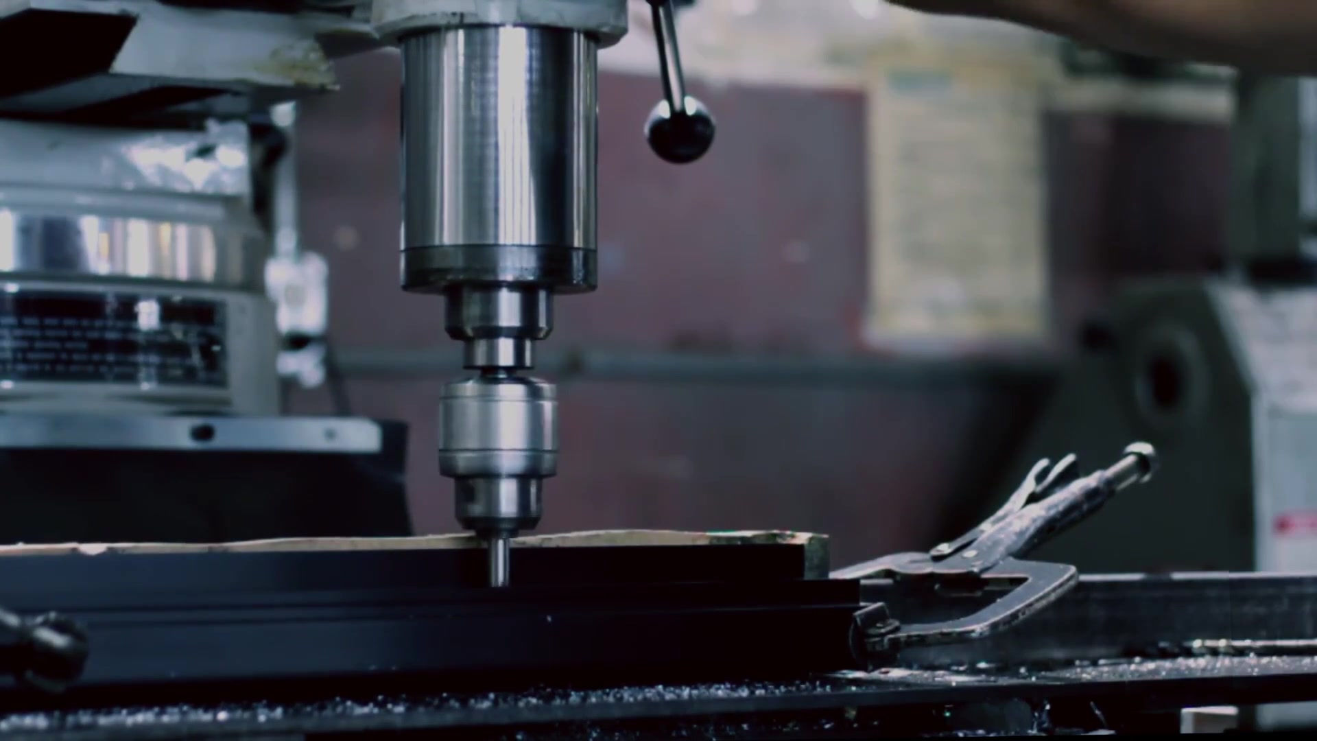
Прилагодено производство на делови, компоненти, склопови, готови производи, машини и индустриска опрема
Домашно и глобално договорно производство
Производство Аутсорсинг
Домашни, глобални набавки на индустриски производи
Приватно означување / Бело означување на вашите производи со вашето име на бренд
Услуги за пронаоѓање и лоцирање производи
Глобален дизајн и партнерство за канали
Инженерска интеграција
Инженерски услуги
Глобална консолидација, складирање, логистика


