

Глобален прилагоден производител, интегратор, консолидатор, партнер за аутсорсинг за широк спектар на производи и услуги.
Ние сме ваш единствен извор за производство, изработка, инженерство, консолидација, интеграција, аутсорсинг на нарачано произведени и производи и услуги кои не се на полица. Ние, исто така, приватна етикета / бела етикета на вашите производи со името на вашиот бренд ако сакате.
Изберете го вашиот јазик
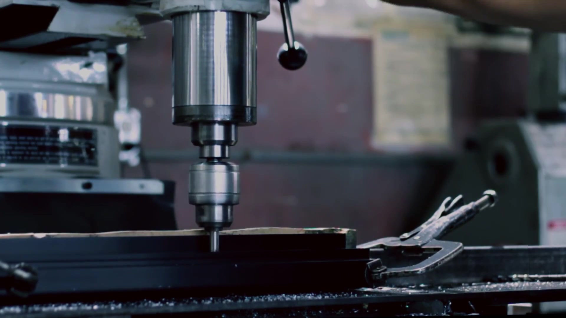
Прилагодено производство на делови, компоненти, склопови, готови производи, машини и индустриска опрема
Домашно и глобално договорно производство
Производство Аутсорсинг
Домашни, глобални набавки на индустриски производи
Приватно означување / Бело означување на вашите производи со вашето име на бренд
Услуги за пронаоѓање и лоцирање производи
Глобален дизајн и партнерство за канали
Инженерска интеграција
Инженерски услуги
Глобална консолидација, складирање, логистика


Search Results
164 results found with an empty search
- Global Product Finder Locator for Off Shelf Products
Global Product Finder Locator for Off Shelf Products AGS-TECH, Inc. е ваш Глобален прилагоден производител, интегратор, консолидатор, аутсорсинг партнер. Ние сме вашиот едношалтерски извор за производство, изработка, инженерство, консолидација, аутсорсинг. Ако точно го знаете производот што го барате, ве молиме пополнете ја табелата подолу Доколку пополнувањето на формуларот подолу не е можно или е премногу тешко, ние го прифаќаме вашето барање и преку е-пошта. Едноставно пишете ни на sales@agstech.net Get a Price Quote on a known brand, model, part number....etc. First name Last name Email Phone Product Name Product Make or Brand Please Enter Manufacturer Part Number if Known Please Enter SKU Code if You Know: Your Application for the Product Quantity Needed Do You have a price target ? If so, please let us know: Give us more details if you want: Condition of Product Needed New Used Does Not Matter Доколку имате такви, поставете ги соодветните датотеки за производот со кликнување на врската подолу. Не грижете се, врската подолу ќе се појави нов прозорец за преземање на вашите датотеки. Нема да се движите подалеку од овој тековен прозорец. Откако ќе ги поставите вашите датотеки, затворете го САМО прозорецот на Dropbox, но не и оваа страница. Погрижете се да ги пополните сите празни места и кликнете на копчето за поднесување подолу. КЛИКНЕТЕ ТУКА ЗА ДА ПОСТАВЕТЕ ДАТОТЕКИ Request a Quote Thanks! We’ll send you a price quote shortly. ПРЕТХОДНА СТРАНИЦА Ние сме AGS-TECH Inc., ваш единствен извор за производство и изработка и инженерство и аутсорсинг и консолидација. Ние сме најразновидниот инженерски интегратор во светот кој ви нуди сопствено производство, подсклопување, склопување на производи и инженерски услуги.
- Custom Made Products Data Entry
Custom Made Products Data Entry, Custom Manufactured Parts, Assemblies, Plastic Molds, Casting, CNC Machining, Extrusion, Metal Forging, Spring Manufacturing, Products Assembly, PCBA, PCB AGS-TECH, Inc. е ваш Глобален прилагоден производител, интегратор, консолидатор, аутсорсинг партнер. Ние сме вашиот едношалтерски извор за производство, изработка, инженерство, консолидација, аутсорсинг. Пополнете ги вашите информации ако ви треба сопствен дизајн и развој и прототипови и масовно производство: Доколку пополнувањето на формуларот подолу не е можно или е премногу тешко, ние го прифаќаме вашето барање и преку е-пошта. Едноставно пишете ни на sales@agstech.net Get a Price Quote on a custom designed, developed, prototyped or manufactured product. First name Last name Email Phone Product Name Your Application for the Product Quantity Needed Do you have a price target ? If you do have, please let us know your expected price: Give us more details if you want: Do you accept offshore manufacturing ? YES NO Доколку имате такви, поставете ги соодветните датотеки за производот со кликнување на врската подолу. Не грижете се, врската подолу ќе се појави нов прозорец за преземање на вашите датотеки. Нема да се движите подалеку од овој тековен прозорец. Откако ќе ги поставите вашите датотеки, затворете го САМО прозорецот на Dropbox, но не и оваа страница. Погрижете се да ги пополните сите празни места и кликнете на копчето за поднесување подолу. Датотеките кои ќе ни помогнат да го цитираме вашиот специјално прилагоден производ се технички цртежи, сметка за материјали, фотографии, скици... итн. Можете да преземете повеќе од една датотека. КЛИКНЕТЕ ТУКА ЗА ДА ПОСТАВЕТЕ ДАТОТЕКИ Request a Quote Thanks! We’ll send you a price quote shortly. ПРЕТХОДНА СТРАНИЦА Ние сме AGS-TECH Inc., ваш единствен извор за производство и изработка и инженерство и аутсорсинг и консолидација. Ние сме најразновидниот инженерски интегратор во светот кој ви нуди сопствено производство, подсклопување, склопување на производи и инженерски услуги.
- Metal Stamping, Sheet Metal Fabrication, Zinc Plated Metal Stamped
Metal Stamping & Sheet Metal Fabrication, Zinc Plated Metal Stamped Parts, Wire and Spring Forming Метално штанцување и изработка на лим Цинк обложени печат делови Прецизни печати и формирање на жица Цинк обложени прилагодени прецизни метални печати Прецизно печатени делови AGS-TECH Inc. прецизно печат на метал Изработка на лим од AGS-TECH Inc. Брзо прототипирање на лим од AGS-TECH Inc. Печатење на подлошки во голем волумен Развој и изработка на куќиште за филтер за масло од лим Изработка на компоненти од лим за филтер за масло и комплетна монтажа Прилагодено изработка и монтажа на производи од лим Изработка на дихтунзи за глава од AGS-TECH Inc. Изработка на заптивки во AGS-TECH Inc. Изработка на куќишта од лим - AGS-TECH Inc Едноставни единечни и прогресивни печати од AGS-TECH Inc. Печати од метал и метални легури - AGS-TECH Inc Метални делови пред завршувањето на работата Формирање лим - Електрично куќиште - AGS-TECH Inc Производство на сечила за сечење обложени со титаниум за прехранбената индустрија Изработка на ножеви за скијање за индустријата за пакување храна PREVIOUS PAGE
- Camera Systems & Components, Optic Scanner, Optical Readers, CCD
Camera Systems - Components - Optic Scanner - Optical Readers - Imaging System - CCD - Optomechanical Systems - IR Cameras Производство и склопување приспособени системи за камера AGS-TECH offers: • Camera systems, camera components and custom camera assemblies • Custom designed and manufactured optical scanners, readers, optical security product assemblies. • Precision optical, opto-mechanical and electro-optical assemblies integrating imaging and nonimaging optics, LED lighting, fiber optics and CCD cameras • Among the products our optical engineers have developed are: - Omni-directional periscope and camera for surveillance and security applications. 360 x 60º field of view high resolution image, no stitching required. - Inner cavity wide angle video camera - Super slim 0.6 mm diameter flexible video endoscope. All medical video couplers fit over standard endoscope eyepieces and are completely sealed and soakable. For our medical endoscope and camera systems, please visit: http://www.agsmedical.com - Video camera and coupler for semi-rigid endoscope - Eye-Q Videoprobe. Non-contact zoom videoprobe for coordinate measuring machines. - Optical spectrograph & IR imaging system (OSIRIS) for ODIN satellite. Our engineers worked on the flight unit assembly, alignment, integration and test. - Wind imaging interferometer (WINDII) for NASA upper atmosphere research satellite (UARS). Our engineers worked on consulting on assembly, integration and test. WINDII performance and operational lifetime far exceeded the design goals and requirements. Depending on your application, we will determine what dimensions, pixel count, resolution, wavelength sensitivity your camera application requires. We can build systems for you suitable for infrared, visible and other wavelengths. Contact us today to find out more. Dowload brochure for our DESIGN PARTNERSHIP PROGRAM Developing a customized camera system can take relatively longer lead times and cost more as compared to ready-to-use systems. Therefore please click on the blue links below to check whether any of our ready-to-use products fit your application: Barcode and Fixed Mount Scanners - RFID Products - Mobile Computers - Micro Kiosks OEM Technology (We private label these with your brand name and logo if you wish) Barcode Scanners (We private label these with your brand name and logo if you wish) Fixed Industrial Scanners (We private label these with your brand name and logo if you wish) Hikrobot Machine Vision Products Hikrobot Smart Machine Vision Products Hikrobot Machine Vision Standard Products Hikvision Logistic Vision Solutions Private Label Medical Endoscopes and Visualization Systems (We can put your company name and logo on these) Also make sure to download our comprehensive electric & electronic components catalog for off-shelf products by CLICKING HERE. КЛИКНЕТЕ Услуга за пронаоѓање на производи-локатор ПРЕТХОДНА СТРАНИЦА
- Plasma Machining, HF Plasma Cutting, Plasma Gouging, CNC, Arc Welding
Plasma Machining - HF Plasma Cutting - Plasma Gouging - CNC - Plasma Arc Welding - PAW - GTAW - AGS-TECH Inc. - New Mexico Плазма обработка и сечење We use the PLASMA CUTTING and PLASMA MACHINING processes to cut and machine steel, aluminum, metals and other materials of different thicknesses using a plasma torch. In plasma-cutting (also sometimes called PLASMA-ARC CUTTING), an inert gas or compressed air is blown at high speed out of a nozzle and simultaneously an electrical arc is formed through that gas from the nozzle to the surface being cut, turning a portion of that gas to plasma. To simplify, plasma can be described as the fourth state of matter. The three states of matter are solid, liquid and gas. For a common example, water, these three states are ice, water and steam. The difference between these states relates to their energy levels. When we add energy in the form of heat to ice, it melts and forms water. When we add more energy, the water vaporizes in the form of steam. By adding more energy to steam these gases become ionized. This ionization process causes the gas to become electrically conductive. We call this electrically conductive, ionized gas a “plasma”. The plasma is very hot and melts the metal being cut and at the same time blowing the molten metal away from the cut. We use plasma for cutting thin and thick, ferrous and nonferrous materials alike. Our hand-held torches can usually cut up to 2 inches thick steel plate, and our stronger computer-controlled torches can cut steel up to 6 inches thick. Plasma cutters produce a very hot and localized cone to cut with, and are therefore very suitable for cutting metal sheets in curved and angled shapes. The temperatures generated in plasma-arc cutting are very high and around 9673 Kelvin in the oxygen plasma torch. This offers us a fast process, small kerf width, and good surface finish. In our systems using tungsten electrodes, the plasma is inert, formed using either argon, argon-H2 or nitrogen gases. However, we also use sometimes oxidizing gases, such as air or oxygen, and in those systems the electrode is copper with hafnium. The advantage of an air plasma torch is that it uses air instead of expensive gases, thus potentially reducing overall cost of machining . Our HF-TYPE PLASMA CUTTING machines use a high-frequency, high-voltage spark to ionize the air through the torch head and initiate arcs. Our HF plasma cutters do not require the torch to be in contact with the workpiece material at the start, and are suitable for applications involving COMPUTER NUMERICAL CONTROL (CNC) cutting. Other manufacturers are using primitive machines that require tip contact with the parent metal to start and then the gap separation occurs. These more primitive plasma cutters are more susceptible to contact tip and shield damage at starting. Our PILOT-ARC TYPE PLASMA machines use a two step process for producing plasma, without the need for initial contact. In the first step, a high-voltage, low current circuit is used to initialize a very small high-intensity spark within the torch body, generating a small pocket of plasma gas. This is called the pilot arc. The pilot arc has a return electrical path built into the torch head. The pilot arc is maintained and preserved until it is brought into proximity of the workpiece. There the pilot arc ignites the main plasma cutting arc. Plasma arcs are extremely hot and are in the range of 25,000 °C = 45,000 °F. A more traditional method we also deploy is OXYFUEL-GAS CUTTING (OFC) where we use a torch as in welding. The operation is used in cutting of steel, cast iron and cast steel. The principle of cutting in oxyfuel-gas cutting is based on oxidation, burning and melting of the steel. Kerf widths in oxyfuel-gas cutting are in the neighborhood of 1.5 to 10mm. The plasma arc process has been seen as an alternative to the oxy-fuel process. The plasma-arc process differs from the oxy-fuel process in that it operates by using the arc to melt the metal whereas in the oxy-fuel process, the oxygen oxidizes the metal and the heat from the exothermic reaction melts the metal. Therefore, unlike the oxy-fuel process, the plasma-process can be applied for cutting metals which form refractory oxides such as stainless steel, aluminium, and non-ferrous alloys. PLASMA GOUGING a similar process to plasma cutting, is typically performed with the same equipment as plasma cutting. Instead of cutting the material, plasma gouging uses a different torch configuration. The torch nozzle and gas diffuser is usually different, and a longer torch-to-workpiece distance is maintained for blowing away metal. Plasma gouging can be used in various applications, including removing a weld for rework. Some of our plasma cutters are built in to the CNC table. CNC tables have a computer to control the torch head to produce clean sharp cuts. Our modern CNC plasma equipment is capable of multi-axis cutting of thick materials and allowing opportunities for complex welding seams that are not possible otherwise. Our plasma-arc cutters are highly automated through the use of programmable controls. For thinner materials, we prefer laser cutting to plasma cutting, mostly because of our laser cutter's superior hole-cutting abilities. We also deploy vertical CNC plasma cutting machines, offering us a smaller footprint, increased flexibility, better safety and faster operation. The quality of the plasma cut edge is similar to that achieved with the oxy-fuel cutting processes. However, because the plasma process cuts by melting, a characteristic feature is the greater degree of melting towards the top of the metal resulting in top edge rounding, poor edge squareness or a bevel on the cut edge. We use new models of plasma torches with a smaller nozzle and a thinner plasma arc to improve arc constriction to produce more uniform heating at the top and bottom of the cut. This allows us to obtain near-laser precision on plasma cut and machined edges. Our HIGH TOLERANCE PLASMA ARC CUTTING (HTPAC) systems operate with a highly constricted plasma. Focusing of the plasma is achieved by forcing the oxygen generated plasma to swirl as it enters the plasma orifice and a secondary flow of gas is injected downstream of the plasma nozzle. We have a separate magnetic field surrounding the arc. This stabilises the plasma jet by maintaining the rotation induced by the swirling gas. By combining precision CNC control with these smaller and thinner torches we are capable to produce parts that require little or no finishing. Material removal rates in plasma-machining are much higher than in the Electric-Discharge-Machining (EDM) and Laser-Beam-Machining (LBM) processes, and parts can be machined with good reproducibility. PLASMA ARC WELDING (PAW) is a process similar to gas tungsten arc welding (GTAW). The electric arc is formed between an electrode generally made of sintered tungsten and the workpiece. The key difference from GTAW is that in PAW, by positioning the electrode within the body of the torch, the plasma arc can be separated from the shielding gas envelope. The plasma is then forced through a fine-bore copper nozzle which constricts the arc and the plasma exiting the orifice at high velocities and temperatures approaching 20,000 °C. Plasma arc welding is an advancement over the GTAW process. The PAW welding process uses a non-consumable tungsten electrode and an arc constricted through a fine-bore copper nozzle. PAW can be used to join all metals and alloys that are weldable with GTAW. Several basic PAW process variations are possible by varying the current, plasma gas flow rate, and the orifice diameter, including: Micro-plasma (< 15 Amperes) Melt-in mode (15–400 Amperes) Keyhole mode (>100 Amperes) In plasma arc welding (PAW) we obtain a greater energy concentration as compared to GTAW. Deep and narrow penetration is achievable, with a maximum depth of 12 to 18 mm (0.47 to 0.71 in) depending on the material. Greater arc stability allows a much longer arc length (stand-off), and much greater tolerance to arc length changes. As a disadvantage however, PAW requires relatively expensive and complex equipment as compared to GTAW. Also the torch maintenance is critical and more challenging. Other disadvantages of PAW are: Welding procedures tend to be more complex and less tolerant to variations in fit-up, etc. Operator skill required is a little more than for GTAW. Orifice replacement is necessary. КЛИКНЕТЕ Услуга за пронаоѓање на производи-локатор ПРЕТХОДНА СТРАНИЦА
- Accessories, Modules, Carrier Boards | agstech
Industrial Computer Accessories, PCI, Peripheral Component Interconnect, Multichannel Analog & Digital Input Output Modules, Relay Module, Printer Interface Додатоци, модули, табли за носачи за индустриски компјутери A PERIPHERAL DEVICE is one attached to a host computer, but not part of it, and is more or less dependent on the host. It expands the host's capabilities, but does not form part of the core computer architecture. Examples are computer printers, image scanners, tape drives, microphones, loudspeakers, webcams, and digital cameras. Peripheral devices connect to the system unit through the ports on the computer. CONVENTIONAL PCI (PCI stands for PERIPHERAL COMPONENT INTERCONNECT, part of the PCI Local Bus standard) is a computer bus for attaching hardware devices in a computer. These devices can take either the form of an integrated circuit fitted onto the motherboard itself, called a planar device in the PCI specification, or an expansion card that fits into a slot. We carry name brands such as JANZ TEC, DFI-ITOX and KORENIX. Click on blue highlighted text to download brochure or catalog: - Catalog for Vandal-Proof IP65/IP67/IP68 Keyboards, Keypads, Pointing Devices, ATM Pinpads, Medical & Military Keyboards and other similar Rugged Computer Peripherals - DFI-ITOX brand Industrial Computer Peripherals - DFI-ITOX brand Graphics Cards - DFI-ITOX brand Industrial Motherboards brochure - DFI-ITOX brand embedded single board computers brochure - DFI-ITOX brand computer-on-board modules brochure - DFI-ITOX brand Embedded OS Services - ICP DAS brand industrial communication and networking products brochure - ICP DAS brand PACs Embedded Controllers & DAQ brochure - ICP DAS brand Industrial Touch Pad brochure - ICP DAS brand Remote IO Modules and IO Expansion Units brochure - ICP DAS brand PCI Boards and IO Cards - JANZ TEC brand compact product brochure - KORENIX brand compact product brochure - Private Label Flash Storage for Embedded Industrial Applications (We can put your name, logo, brand on these.............) To choose a suitable component or accessory for your projects. please go to our industrial computer store by CLICKING HERE. Dowload brochure for our DESIGN PARTNERSHIP PROGRAM Some of the components and accessories we offer for industrial computers are: - Multichannel analog and digital input output modules : We offer hundreds of different 1-, 2-, 4-, 8-, 16-channel function modules. They do have compact size and this small size makes these systems easy to use in confined places. Up to 16 channels can be accommodated in a 12mm (0.47in) wide module. Connections are pluggable, secure and strong, making replacing easy for the operators while the spring pressure technology assures continuous operation even under severe environmental conditions such as shock/vibration, temperature cycling….etc. Our multichannel analog and digital input output modules are highly flexible that each node in the I/O system can be configured to meet each channel’s requirements, digital and analog I/O and others can be easily combined. They are easy to handle, the modular rail-mounted module design allows easy and tool-free handling and modifications. Using colored markers the functionality of individual I/O modules is identified, terminal assignment and technical data are printed onto the side of the module. Our modular systems are fieldbus-independent. - Multichannel relay modules : A relay is a switch controlled by an electric current. Relays make it possible for a low voltage low current circuit to switch a high voltage / high current device safely. As an example, we can use a battery powered small light detector circuit to control large mains powered lights using a relay. Relay boards or modules are commercial circuit boards fitted with relays, LED indicators, back EMF preventing diodes and practical screw-in terminal connections for voltage inputs, NC, NO, COM connections on the relay at the least. Multiple poles on them make it possible to switch multiple devices on or off simultaneously. Most industrial projects require more than one relay. Therefore multi-channel or also known as multiple relay boards are offered. They can have anywhere from 2 to 16 relays on the same circuit board. Relay boards can also be computer controlled directly by USB or serial connection. Relay boards connected to LAN or internet connected PC, we can control relays remotely from far away distances using special software. - Printer interface: A printer interface is a combination of hardware and software that allows the printer to communicate with a computer. The hardware interface is called port and each printer has at least one interface. An interface incorporates several components including its communication type and the interface software. There are eight major communication types: 1. Serial : Through serial connections computers send one bit of information at a time, one after another. Communication parameters such as parity, baud should be set on both entities before communication takes place. 2. Parallel : Parallel communication is more popular with printers because it is faster compared to serial communication. Using parallel type communication, printers receive eight bits at a time over eight separate wires. Parallel uses a DB25 connection on the computer side and an oddly shaped 36 pin connection on the printer side. 3. Universal Serial Bus (popularly referred to as USB) : They can transfer data fast with a transfer rate of up to 12 Mbps and automatically recognize new devices. 4. Network : Also commonly referred to as Ethernet, network connections are commonplace on network laser printers. Other types of printers also employ this type of connection. These printers have a Network Interface Card (NIC) and ROM-based software that allows them to communicate with networks, servers and workstations. 5. Infrared : Infrared transmissions are wireless transmissions that use infrared radiation of the electromagnetic spectrum. An Infrared acceptor allows your devices (laptops, PDA’s, Cameras, etc) connect to the printer and send print commands through infrared signals. 6. Small Computer System Interface (known as SCSI) : Laser printers and some others use SCSI interfaces to PC as there is the benefit of daisy chaining wherein multiple devices could be on a single SCSI connection. Its implementation is easy. 7. IEEE 1394 Firewire : Firewire is a high speed connection widely used for digital video editing and other high bandwidth requirements. This interface currently supports devices with a maximum throughput of 800 Mbps and capable of speeds up to 3.2 Gbps. 8. Wireless : Wireless is the currently popular technology like infrared and bluetooth. The information is transmitted wirelessly through the air using radio waves and is received by the device. Bluetooth is used to replace the cables between computers and its peripherals and they usually work over small distances of about 10 meters. Out of these above communication types scanners mostly use USB, Parallel, SCSI, IEEE 1394/FireWire. - Incremental Encoder Module : Incremental encoders are used in positioning and motor speed feedback applications. Incremental encoders provide excellent speed and distance feedback. As few sensors are involved, the incremental encoder systems are simple and economical. An incremental encoder is limited by only providing change information and therefore the encoder requires a reference device to calculate motion. Our incremental encoder modules are versatile and customizable to fit a variety of applications such as heavy duty applications as is the case in pulp & paper, steel industries; industrial duty applications such as textile, food, beverage industries and light duty/servo applications such as robotics, electronics, semiconductor industry. - Full-CAN Controller For MODULbus Sockets : The Controller Area Network, abbreviated as CAN was introduced to address the growing complexity of vehicle functions and networks. In the first embedded systems, modules contained a single MCU, performing a single or multiple simple functions such as reading a sensor level via an ADC and controlling a DC motor. As functions became more complex, designers adopted distributed module architectures, implementing functions in multiple MCUs on the same PCB. According to this example, a complex module would have the main MCU performing all system functions, diagnostics, and failsafe, while another MCU would handle a BLDC motor control function. This was made possible with the wide availability of general purpose MCUs at a low cost. In today’s vehicles, as functions become distributed within a vehicle rather than a module, the need for a high fault tolerance, inter module communication protocol led to the design and introduction of CAN in the automotive market. Full CAN Controller provides an extensive implementation of message filtering, as well as message parsing in the hardware, thus releasing the CPU from the task of having to respond to every received message. Full CAN controllers can be configured to interrupt the CPU only when messages whose Identifiers have been setup as acceptance filters in the controller. Full CAN controllers are also setup with multiple message objects referred to as mailboxes, which can store specific message information such as ID and data bytes received for the CPU to retrieve. The CPU in this case would retrieve the message any time, however, must complete the task prior to an update of that same message is received and overwrites the current content of the mailbox. This scenario is resolved in the final type of CAN controllers. Extended Full CAN controllers provide an additional level of hardware implemented functionality, by providing a hardware FIFO for received messages. Such an implementation allows more than one instance of the same message to be stored before the CPU is interrupted therefore preventing any information loss for high frequency messages, or even allowing the CPU to focus on the main module function for a longer period of time. Our Full-CAN Controller for MODULbus Sockets offers the following features: Intel 82527 Full CAN controller, Supports CAN protocol V 2.0 A and A 2.0 B, ISO/DIS 11898-2, 9-pin D-SUB connector, Options Isolated CAN interface, Supported Operating Systems are Windows, Windows CE, Linux, QNX, VxWorks. - Intelligent CAN Controller For MODULbus Sockets : We offer our clients local intelligence with MC68332, 256 kB SRAM / 16 bit wide, 64 kB DPRAM / 16 bit wide, 512 kB flash, ISO/DIS 11898-2, 9-pin D-SUB connector, ICANOS firmware on-board, MODULbus+ compatible, options such as isolated CAN interface, CANopen available, operating systems supported are Windows, Windows CE, Linux, QNX, VxWorks. - Intelligent MC68332 Based VMEbus Computer : VMEbus standing for VersaModular Eurocard bus is a computer data path or bus system that is used in industrial, commercial and military applications worldwide. VMEbus is used in traffic control systems, weapons control systems, telecommunication systems, robotics, data acquisition, video imaging...etc. VMEbus systems withstand shock, vibration and extended temperatures better than the standard bus systems used in desktop computers. This makes them ideal for harsh environments. Double euro-card from factor (6U) , A32/24/16:D16/08 VMEbus master; A24:D16/08 slave interface, 3 MODULbus I/O sockets, front-panel and P2 connection of MODULbus I/O lines, programmable MC68332 MCU with 21 MHz, on-board system controller with first slot detection, interrupt handler IRQ 1 – 5, interrupt generator any 1 of 7, 1 MB SRAM main memory, up to 1 MB EPROM, up to1 MB FLASH EPROM, 256 kB dual-ported battery buffered SRAM, battery buffered realtime clock with 2 kB SRAM, RS232 serial port , periodic interrupt timer (internal to MC68332), watchdog timer (internal to MC68332), DC/DC converter to supply analog modules. Options are 4 MB SRAM main memory. Supported operating system is VxWorks. - Intelligent PLC Link Concept (3964R) : A programmable logic controller or briefly PLC is a digital computer used for automation of industrial electromechanical processes, such as control of machinery on factory assembly lines and amusement rides or light fixtures. PLC Link is a protocol to share easily memory area between two PLC’s. The big advantage of PLC Link is to work with PLC’s as Remote I/O units. Our Intelligent PLC Link Concept offers communication procedure 3964®, a messaging interface between host and firmware through software driver, applications on the host to communicate with another station on the seriel line connection, serial data communication according to 3964® protocol, availability of software drivers for various operating systems. - Intelligent Profibus DP Slave Interface : ProfiBus is a messaging format specifically designed for high-speed serial I/O in factory and building automation applications. ProfiBus is an open standard and is recognized as the fastest FieldBus in operation today, based on RS485 and the European EN50170 Electrical Specification. The DP suffix refers to ''Decentralized Periphery'', which is used to describe distributed I/O devices connected via a fast serial data link with a central controller. To the contrary, a programmable logic controller, or PLC described above normally has its input/output channels arranged centrally. By introducing a network bus between the main controller (master) and its I/O channels (slaves), we have decentralized the I/O. A ProfiBus system uses a bus master to poll slave devices distributed in multi-drop fashion on an RS485 serial bus. A ProfiBus slave is any peripheral device (such as an I/O transducer, valve, network drive, or other measuring device) which processes information and sends its output to the master. The slave is a passively operating station on the network since it does not have bus access rights and can only acknowledge received messages, or send response messages to the master upon request. It is important to note that all ProfiBus slaves have the same priority, and that all network communication originates from the master. To summarize: A ProfiBus DP is an open standard based on EN 50170, it is the fastest Fieldbus standard to date with data rates up to 12 Mb, offers plug and play operation, enables up to 244 bytes of input/output data per message, up to 126 stations may connect to the bus and up to 32 stations per bus segment. Our Intelligent Profibus DP Slave Interface Janz Tec VMOD-PROFoffers all functions for motor controlling of DC servo motors, programmable digital PID filter, velocity, target position and filter parameters that are changeable during motion, quadrature encoder interface with pulse input, programmable host interrupts, 12 bit D/A converter, 32 bit position, velocity and acceleration registers. It support Windows, Windows CE, Linux, QNX and VxWorks operating systems. - MODULbus Carrier Board for 3 U VMEbus Systems : This system offers 3 U VMEbus non-intelligent carrier board for MODULbus, single euro-card form factor (3 U), A24/16:D16/08 VMEbus slave interface, 1 socket for MODULbus I/O, jumper selectable interrupt level 1 – 7 and vector-interrupt, short-I/O or standard-addressing, needs only one VME-slot, supports MODULbus+identification mechanism, front panel connector of I/O signals (provided by modules). Options are DC/DC converter for analog module power supply. Supported operating systems are Linux, QNX, VxWorks. - MODULbus Carrier Board For 6 U VMEbus Systems : This system offers 6U VMEbus non-intelligent carrier board for MODULbus, double euro-card, A24/D16 VMEbus slave interface, 4 plug-in sockets for MODULbus I/O, different vector from each MODULbus I/O, 2 kB short-I/O or standard-address range, needs only one VME-slot, front panel and P2 connection of I/O lines. Options are DC/DC converter to supply analog modules power. Supported operating systems are Linux, QNX, VxWorks. - MODULbus Carrier Board For PCI Systems : Our MOD-PCI carrier boards offer non-intelligent PCI with two MODULbus+ sockets, extended height short form factor, 32 bit PCI 2.2 target interface (PLX 9030), 3.3V / 5V PCI interface, only one PCI-bus slot occupied, front panel connector of MODULbus socket 0 available at PCI bus bracket. On the other hand, our MOD-PCI4 boards have non-Intelligent PCI-bus carrier board with four MODULbus+ sockets, extended height long form factor, 32 bit PCI 2.1 target interface (PLX 9052), 5V PCI interface, only one PCI slot occupied, front panel connector of MODULbus socket 0 available at ISAbus bracket, I/O connector of MODULbus socket 1 available on 16-pin flat cable connector at ISA bracket. - Motor Controller For DC Servo Motors : Mechanical systems manufacturers, power & energy equipment producers, transportation & traffic equipment producers and service companies, automotive, medical and many other areas can use our equipment with peace of mind, because we offer robust, reliable and scalable hardware for their drive technology. The modular design of our motor controllers enables us to offer solutions based on emPC systems that are highly flexible and ready to be adapted to customer’s requirements. We are able to design interfaces that are economical and suitable for applications ranging from simple single axis to multiple synchronized axes. Our modular and compact emPCs can be complemented with our scalable emVIEW displays (currently from 6.5” to 19”) for a broad spectrum of applications ranging from simple control systems to integral operator interface systems. Our emPC systems are available in different performance classes and sizes. They have no fans and work with compact-flash media. Our emCONTROL soft PLC environment can be used as a fully fledged, real-time control system enabling both simple as well as complex DRIVE ENGINEERING tasks to be accomplished. We also customize our emPC to meet your specific requirements. - Serial Interface Module : A Serial Interface Module is a device that creates an addressable zone input for a conventional detection device. It offers a connection to an addressable bus, and a supervised zone input. When the zone input is open, the module sends status data to the control panel indicating the open position. When the zone input is shorted, the module sends status data to the control panel, indicating the shorted condition. When the zone input is normal, the module sends data to the control panel, indicating the normal condition. Users see status and alarms from the sensor at the local keypad. The control panel can also send a message to the monitoring station. The serial interface module can be used in alarm systems, building control and energy management systems. Serial interface modules provide important advantages reducing installation labor by its special designs, by providing an addressable zone input, reducing the overall cost of the entire system. Cabling is minimal because the module’s data cable need not be individually routed to the control panel. The cable is an addressable bus that allows connection to many devices before cabling and connecting to the control panel for processing. It saves current, and minimizes the need for additional power supplies because of its low current requirements. - VMEbus Prototyping Board : Our VDEV-IO boards offer double Eurocard form factor (6U) with VMEbus interface, A24/16:D16 VMEbus slave interface, full interruption capabilities, pre-decoding of 8 address ranges, vector register, large matrix field with surrounding track for GND/Vcc, 8 user definable LEDs at the front panel. КЛИКНЕТЕ Услуга за пронаоѓање на производи-локатор ПРЕТХОДНА СТРАНИЦА
- Electric Discharge Machining, EDM, Spark Machining, Die Sinking
Electric Discharge Machining - EDM - Spark Machining - Die Sinking - Wire Erosion - Custom Manufacturing - AGS-TECH Inc. EDM обработка, глодање и мелење со електрично празнење ELECTRICAL DISCHARGE MACHINING (EDM), also referred to as SPARK-EROSION or ELECTRODISCHARGE MACHINING, SPARK ERODING, DIE SINKING or WIRE EROSION, is a NON-CONVENTIONAL MANUFACTURING process where erosion of metals takes place and desired shape is obtained using electrical discharges in the form of sparks. We also offer some varieties of EDM, namely NO-WEAR EDM, WIRE EDM (WEDM), EDM GRINDING (EDG), DIE-SINKING EDM, ELECTRICAL-DISCHARGE MILLING, micro-EDM, m-EDM and ELECTROCHEMICAL-DISCHARGE GRINDING (ECDG). Our EDM systems consist of shaped tools/electrode and the workpiece connected to DC power supplies and inserted in a electrically nonconducting dielectric fluid. After 1940 electrical discharge machining has become one of the most important and popular production technologies in manufacturing industries. When the distance between the two electrodes is reduced, the intensity of the electric field in the volume between the electrodes becomes greater than the strength of the dielectric in some points, which breaks, eventually forming a bridge for current to flow between the two electrodes. An intense electrical arc is generated causing significant heating to melt a portion of the workpiece and some of the tooling material. As a result, material is removed from both the electrodes. At the same time, the dielectric fluid is heated rapidly, resulting in evaporation of the fluid in the arc gap. Once the current flow stops or it is stopped heat is removed from the gas bubble by the surrounding dielectric fluid and the bubble cavitates (collapses). The shock wave created by the bubble’s collapse and the flow of dielectric fluid flush debris from the workpiece surface and entrain any molten workpiece material into the dielectric fluid. The repetition rate for these discharges are between 50 to 500 kHz, voltages between 50 to 380 V and currents between 0.1 and 500 Amperes. New liquid dielectric such as mineral oils, kerosene or distilled & deionized water is usually conveyed into the inter-electrode volume carrying away the solid particles (in the form of debris) and the insulating proprieties of the dielectric is restored. After a current flow, the potential difference between the two electrodes is restored to what it was before the breakdown, so a new liquid dielectric breakdown can occur. Our modern electrical discharge machines (EDM) offer numerically controlled movements and are equipped with pumps and filtering systems for the dielectric fluids. Electrical discharge machining (EDM) is a machining method mainly used for hard metals or those that would be very difficult to machine with conventional techniques. EDM typically works with any materials that are electrical conductors, although methods for machining insulating ceramics with EDM have also been proposed. The melting point and latent heat of melting are properties that determine the volume of metal removed per discharge. The higher these values, the slower the material removal rate. Because the electrical discharge machining process does not involve any mechanical energy, the hardness, strength, and toughness of the workpiece do not affect the removal rate. Discharge frequency or energy per discharge, the voltage and current are varied to control material removal rates. Rate of material removal and surface roughness increase with increasing current density and decreasing spark frequency. We can cut intricate contours or cavities in pre-hardened steel using EDM without the need for heat treatment to soften and re-harden them. We can use this method with any metal or metal alloys like titanium, hastelloy, kovar, and inconel. Applications of the EDM process include shaping of polycrystalline diamond tools. EDM is considered a non-traditional or non-conventional machining method along with processes such as electrochemical machining (ECM), water jet cutting (WJ, AWJ), laser cutting. On the other hand the conventional machining methods include turning, milling, grinding, drilling and other process whose material removal mechanism is essentially based on mechanical forces. Electrodes for electrical-discharge machining (EDM) are made of graphite, brass, copper and copper-tungsten alloy. Electrode diameters down to 0.1mm are possible. Since tool wear is an undesired phenomenon adversely affecting dimensional accuracy in EDM, we take advantage of a process called NO-WEAR EDM, by reversing polarity and using copper tools to minimize tool wear. Ideally speaking, the electrical-discharge machining (EDM) can be considered a series of breakdown and restoration of the dielectric liquid between the electrodes. In reality however, the removal of the debris from the inter-electrode area is almost always partial. This causes the electrical proprieties of the dielectric in the inter-electrodes area to be different from their nominal values and vary with time. The inter-electrode distance, (spark-gap), is adjusted by the control algorithms of the specific machine used. The spark-gap in EDM can unfortunately sometimes be short-circuited by the debris. The control system of the electrode may fail to react quickly enough to prevent the two electrodes (tool and workpiece) from short circuiting. This unwanted short circuit contributes to material removal differently from the ideal case. We pay utmost importance to flushing action in order to restore the insulating properties of the dielectric so that the current always happens in the point of the inter-electrode area, thereby minimizing the possibility of unwanted change of shape (damage) of the tool-electrode and workpiece. To obtain a specific geometry, the EDM tool is guided along the desired path very close to the workpiece without touching it, We pay utmost attention to the performance of motion control in use. This way, a large number of current discharges / sparks take place, and each contributes to the removal of material from both tool and workpiece, where small craters are formed. The size of the craters is a function of the technological parameters set for the specific job at hand and dimensions may range from the nanoscale (such as in the case of micro-EDM operations) to some hundreds of micrometers in roughing conditions. These small craters on the tool cause gradual erosion of the electrode called “tool wear”. To counteract the detrimental effect of the wear on the geometry of the workpiece we continuously replace the tool-electrode during a machining operation. Sometimes we achieve this by using a continuously replaced wire as electrode ( this EDM process is also called WIRE EDM ). Sometimes we use the tool-electrode in such a way that only a small portion of it is actually engaged in the machining process and this portion is changed on a regular basis. This is, for instance, the case when using a rotating disk as a tool-electrode. This process is called EDM GRINDING. Yet another technique we deploy consists of using a set of electrodes with different sizes and shapes during the same EDM operation to compensate for wear. We call this multiple electrode technique, and is most commonly used when the tool electrode replicates in negative the desired shape and is advanced towards the blank along a single direction, usually the vertical direction (i.e. z-axis). This resembles the sink of the tool into the dielectric liquid in which the workpiece is immersed, and therefore it is referred to as DIE-SINKING EDM (sometimes called CONVENTIONAL EDM or RAM EDM). The machines for this operation are called SINKER EDM. The electrodes for this type of EDM have complex forms. If the final geometry is obtained using a usually simple-shaped electrode moved along several directions and is also subject to rotations, we call it EDM MILLING. The amount of wear is strictly dependent on the technological parameters used in the operation ( polarity, maximum current, open circuit voltage). For example, in micro-EDM, also known as m-EDM, these parameters are usually set at values which generates severe wear. Therefore, wear is a major problem in that area which we minimize using our accumulated know-how. For example to minimize wear to graphite electrodes, a digital generator, controllable within milliseconds, reverses polarity as electro-erosion takes place. This results in an effect similar to electroplating that continuously deposits the eroded graphite back on the electrode. In another method, a so-called ''Zero Wear'' circuit we minimize how often the discharge starts and stops, keeping it on for as long a time as possible. The material removal rate in electrical-discharge machining can be estimated from: MRR = 4 x 10 exp(4) x I x Tw exp (-1.23) Here MRR is in mm3/min, I is current in Amperes, Tw is workpiece melting point in K-273.15K. The exp stands for exponent. On the other hand, the wear rate Wt of the electrode can be obtained from: Wt = ( 1.1 x 10exp(11) ) x I x Ttexp(-2.38) Here Wt is in mm3/min and Tt is melting point of the electrode material in K-273.15K Finally, the wear ratio of the workpiece to electrode R can be obtained from: R = 2.25 x Trexp(-2.38) Here Tr is the ratio of melting points of workpiece to electrode. SINKER EDM : Sinker EDM, also referred to as CAVITY TYPE EDM or VOLUME EDM, consists of an electrode and workpiece submerged in an insulating liquid. The electrode and workpiece are connected to a power supply. The power supply generates an electrical potential between the two. As the electrode approaches the workpiece, dielectric breakdown occurs in the fluid, forming a plasma channel, and a small spark jumps. The sparks usually strike one at a time because it is highly unlikely that different locations in the inter-electrode space have identical local electrical characteristics which would enable a spark to occur in all such locations simultaneously. Hundreds of thousands of these sparks happen at random points between the electrode and the workpiece per second. As the base metal erodes, and the spark gap subsequently increases, the electrode is lowered automatically by our CNC machine so that the process can continue uninterrupted. Our equipment has controlling cycles known as ''on time'' and ''off time''. The on time setting determines the length or duration of the spark. A longer on time produces a deeper cavity for that spark and all subsequent sparks for that cycle, creating a rougher finish on the workpiece and vice versa. The off time is the period of time that one spark is replaced by another. A longer off time permits the dielectric fluid to flush through a nozzle to clean out the eroded debris, thereby avoiding a short circuit. These settings are adjusted in micro seconds. WIRE EDM : In WIRE ELECTRICAL DISCHARGE MACHINING (WEDM), also called WIRE-CUT EDM or WIRE CUTTING, we feed a thin single-strand metal wire of brass through the workpiece, which is submerged in a tank of dielectric fluid. Wire EDM is an important variation of EDM. We occasionally use wire-cut EDM to cut plates as thick as 300mm and to make punches, tools, and dies from hard metals that are difficult to machine with other manufacturing methods. In this process which resembles to contour cutting with a band saw, the wire, which is constantly fed from a spool, is held between upper and lower diamond guides. The CNC-controlled guides move in the x–y plane and the upper guide can also move independently in the z–u–v axis, giving rise to the ability to cut tapered and transitioning shapes (such as circle on the bottom and square at the top). The upper guide can control axis movements in x–y–u–v–i–j–k–l–. This allows the WEDM to cut very intricate and delicate shapes. The average cutting kerf of our equipment that achieves the best economic cost and machining time is 0.335 mm using Ø 0.25 brass, copper or tungsten wire. However the upper and lower diamond guides of our CNC equipment are accurate to about 0.004 mm, and can have a cutting path or kerf as small as 0.021 mm using Ø 0.02 mm wire. So really narrow cuts are possible. The cutting width is greater than the width of the wire because sparking occurs from the sides of the wire to the workpiece, causing erosion. This ''overcut'' is necessary, for many applications it is predictable and therefore can be compensated for ( in micro-EDM this is not often the case). The wire spools are long—an 8 kg spool of 0.25 mm wire is just over 19 kilometers in length. Wire diameter can be as small as 20 micrometres and the geometry precision is in the neighborhood of +/- 1 micrometer. We generally use the wire only once and recycle it because it is relatively inexpensive. It travels at a constant velocity of 0.15 to 9m/min and a constant kerf (slot) is maintained during a cut. In the wire-cut EDM process we use water as the dielectric fluid, controlling its resistivity and other electrical properties with filters and de-ionizer units. The water flushes the cut debris away from the cutting zone. Flushing is an important factor in determining the maximum feed rate for a given material thickness and therefore we keep it consistent. Cutting speed in wire EDM is stated in terms of the cross-sectional area cut per unit time, such as 18,000 mm2/hr for 50mm thick D2 tool steel. The linear cutting speed for this case would be 18,000/50 = 360mm/hr The material removal rate in wire EDM is: MRR = Vf x h x b Here MRR is in mm3/min, Vf is the feed rate of the wire into workpiece in mm/min, h is thickness or height in mm, and b is the kerf, which is: b = dw + 2s Here dw is wire diameter and s is gap between wire and workpiece in mm. Along with tighter tolerances, our modern multi axis EDM wire-cutting machining centers have added features such as multi heads for cutting two parts at the same time, controls for preventing wire breakage, automatic self-threading features in case of wire breakage, and programmed machining strategies to optimize the operation, straight and angular cutting capabilities. Wire-EDM offers us low residual stresses, because it does not require high cutting forces for removal of material. When the energy/power per pulse is relatively low (as in finishing operations), little change in the mechanical properties of a material is expected due to low residual stresses. ELECTRICAL-DISCHARGE GRINDING (EDG) : The grinding wheels do not contain abrasives, they are made of graphite or brass. Repetitive sparks between the rotating wheel and workpiece remove material from workpiece surfaces. The material removal rate is: MRR = K x I Here MRR is in mm3/min, I is current in Amperes, and K is workpiece material factor in mm3/A-min. We frequently use electrical-discharge grinding to saw narrow slits on components. We sometimes combine EDG (Electrical-Discharge Grinding) process with ECG (Electrochemical Grinding) process where material is removed by chemical action, the electrical discharges from the graphite wheel breaking up the oxide film and washed away by the electrolyte. The process is called ELECTROCHEMICAL-DISCHARGE GRINDING (ECDG). Even though the ECDG process consumes relatively more power, it is a faster process than the EDG. We mostly grind carbide tools using this technique. Applications of Electrical Discharge Machining: Prototype production: We use the EDM process in mold-making, tool and die manufacturing, as well as for making prototype and production parts, especially for the aerospace, automobile and electronics industries in which production quantities are relatively low. In Sinker EDM, a graphite, copper tungsten or pure copper electrode is machined into the desired (negative) shape and fed into the workpiece on the end of a vertical ram. Coinage die making: For the creation of dies for producing jewelry and badges by the coinage (stamping) process, the positive master may be made from sterling silver, since (with appropriate machine settings) the master is significantly eroded and is used only once. The resultant negative die is then hardened and used in a drop hammer to produce stamped flats from cutout sheet blanks of bronze, silver, or low proof gold alloy. For badges these flats may be further shaped to a curved surface by another die. This type of EDM is usually performed submerged in an oil-based dielectric. The finished object may be further refined by hard (glass) or soft (paint) enameling and/or electroplated with pure gold or nickel. Softer materials such as silver may be hand engraved as a refinement. Drilling of Small Holes: On our wire-cut EDM machines, we use small hole drilling EDM to make a through hole in a workpiece through which to thread the wire for the wire-cut EDM operation. Separate EDM heads specifically for small hole drilling are mounted on our wire-cut machines which allow large hardened plates to have finished parts eroded from them as needed and without pre-drilling. We also use small hole EDM to drill rows of holes into the edges of turbine blades used in jet engines. Gas flow through these small holes allows the engines to use higher temperatures than otherwise possible. The high-temperature, very hard, single crystal alloys these blades are made of makes conventional machining of these holes with high aspect ratio extremely difficult and even impossible. Other application areas for small hole EDM is to create microscopic orifices for fuel system components. Besides the integrated EDM heads, we deploy stand-alone small hole drilling EDM machines with x–y axes to machine blind or through holes. EDM drills bore holes with a long brass or copper tube electrode that rotates in a chuck with a constant flow of distilled or deionized water flowing through the electrode as a flushing agent and dielectric. Some small-hole drilling EDMs are able to drill through 100 mm of soft or even hardened steel in less than 10 seconds. Holes between 0.3 mm and 6.1 mm can be achieved in this drilling operation. Metal disintegration machining: We also have special EDM machines for the specific purpose of removing broken tools (drill bits or taps) from work pieces. This process is called ''metal disintegration machining''. Advantages and Disadvantages Electrical-Discharge Machining: Advantages of EDM include machining of: - Complex shapes that would otherwise be difficult to produce with conventional cutting tools - Extremely hard material to very close tolerances - Very small work pieces where conventional cutting tools may damage the part from excess cutting tool pressure. - There is no direct contact between tool and work piece. Therefore delicate sections and weak materials can be machined without any distortion. - A good surface finish can be obtained. - Very fine holes can be easily drilled. Disadvantages of EDM include: - The slow rate of material removal. - The additional time and cost used for creating electrodes for ram/sinker EDM. - Reproducing sharp corners on the workpiece is difficult due to electrode wear. - Power consumption is high. - ''Overcut'' is formed. - Excessive tool wear occurs during machining. - Electrically non-conductive materials can be machined only with specific set-up of the process. КЛИКНЕТЕ Услуга за пронаоѓање на производи-локатор ПРЕТХОДНА СТРАНИЦА
- Microelectronics Manufacturing, Semiconductor Fabrication, Foundry, IC
Microelectronics Manufacturing, Semiconductor Fabrication - Foundry - FPGA - IC Assembly Packaging - AGS-TECH Inc. Микроелектроника и производство и производство на полупроводници Many of our nanomanufacturing, micromanufacturing and mesomanufacturing techniques and processes explained under the other menus can be used for MICROELECTRONICS MANUFACTURING too. However due to the importance of microelectronics in our products, we will concentrate on the subject specific applications of these processes here. Microelectronics related processes are also widely referred to as SEMICONDUCTOR FABRICATION processes. Our semiconductor engineering design and fabrication services include: - FPGA board design, development and programming - Microelectronics foundry services: Design, prototyping and manufacturing, third-party services - Semiconductor wafer preparation: Dicing, backgrinding, thinning, reticle placement, die sorting, pick and place, inspection - Microelectronic package design and fabrication: Both off-shelf and custom design and fabrication - Semiconductor IC assembly & packaging & test: Die, wire and chip bonding, encapsulation, assembly, marking and branding - Lead frames for semiconductor devices: Both off-shelf and custom design and fabrication - Design and fabrication of heat sinks for microelectronics: Both off-shelf and custom design and fabrication - Sensor & actuator design and fabrication: Both off-shelf and custom design and fabrication - Optoelectronic & photonic circuits design and fabrication Let us examine the microelectronics and semiconductor fabrication and test technologies in more detail so you can better understand the services and products we are offering. FPGA Board Design & Development and Programming: Field-programmable gate arrays (FPGAs) are reprogrammable silicon chips. Contrary to processors that you find in personal computers, programming an FPGA rewires the chip itself to implement user’s functionality rather than running a software application. Using prebuilt logic blocks and programmable routing resources, FPGA chips can be configured to implement custom hardware functionality without using a breadboard and soldering iron. Digital computing tasks are carried out in software and compiled down to a configuration file or bitstream that contains information on how the components should be wired together. FPGAs can be used to implement any logical function that an ASIC could perform and are completely reconfigurable and can be given a completely different “personality” by recompiling a different circuit configuration. FPGAs combine the best parts of application-specific integrated circuits (ASICs) and processor-based systems. These benefits include the following: • Faster I/O response times and specialized functionality • Exceeding the computing power of digital signal processors (DSPs) • Rapid prototyping and verification without the fabrication process of custom ASIC • Implementation of custom functionality with the reliability of dedicated deterministic hardware • Field-upgradable eliminating the expense of custom ASIC re-design and maintenance FPGAs provide speed and reliability, without requiring high volumes to justify the large upfront expense of custom ASIC design. Reprogrammable silicon also has the same flexibility of software running on processor-based systems, and it is not limited by the number of processing cores available. Unlike processors, FPGAs are truly parallel in nature, so different processing operations do not have to compete for the same resources. Each independent processing task is assigned to a dedicated section of the chip, and can function autonomously without any influence from other logic blocks. As a result, the performance of one part of the application is not affected when more processing is added on. Some FPGAs have analog features in addition to digital functions. Some common analog features are programmable slew rate and drive strength on each output pin, allowing the engineer to set slow rates on lightly loaded pins that would otherwise ring or couple unacceptably, and to set stronger, faster rates on heavily loaded pins on high-speed channels that would otherwise run too slowly. Another relatively common analog feature is differential comparators on input pins designed to be connected to differential signaling channels. Some mixed signal FPGAs have integrated peripheral analog-to-digital converters (ADCs) and digital-to-analog converters (DACs) with analog signal conditioning blocks that allow them to operate as a system-on-a-chip. Briefly, the top 5 benefits of FPGA chips are: 1. Good Performance 2. Short Time to Market 3. Low Cost 4. High Reliability 5. Long-Term Maintenance Capability Good Performance – With their capability of accommodating parallel processing, FPGAs have better computing power than digital signal processors (DSPs) and do not require sequential execution as DSPs and can accomplish more per clock cycles. Controlling inputs and outputs (I/O) at the hardware level provides faster response times and specialized functionality to closely match application requirements. Short Time to market - FPGAs offer flexibility and rapid prototyping capabilities and thus shorter time-to-market. Our customers can test an idea or concept and verify it in hardware without going through the long and expensive fabrication process of custom ASIC design. We can implement incremental changes and iterate on an FPGA design within hours instead of weeks. Commercial off-the-shelf hardware is also available with different types of I/O already connected to a user-programmable FPGA chip. The growing availability of high-level software tools offer valuable IP cores (prebuilt functions) for advanced control and signal processing. Low Cost—The nonrecurring engineering (NRE) expenses of custom ASIC designs exceed that of FPGA-based hardware solutions. The large initial investment in ASICs can be justified for OEMs producing many chips per year, however many end users need custom hardware functionality for the many systems in development. Our programmable silicon FPGA offers you something with no fabrication costs or long lead times for assembly. System requirements frequently change over time, and the cost of making incremental changes to FPGA designs is negligible when compared to the large expense of respinning an ASIC. High Reliability - Software tools provide the programming environment and FPGA circuitry is a true implementation of program execution. Processor-based systems generally involve multiple layers of abstraction to help task scheduling and share resources among multiple processes. The driver layer controls hardware resources and the OS manages memory and processor bandwidth. For any given processor core, only one instruction can execute at a time, and processor-based systems are continually at risk of time-critical tasks preempting one another. FPGAs, do not use OSs, pose minimum reliability concerns with their true parallel execution and deterministic hardware dedicated to every task. Long-term Maintenance Capability - FPGA chips are field-upgradable and do not require the time and cost involved with redesigning ASIC. Digital communication protocols, for example, have specifications that can change over time, and ASIC-based interfaces may cause maintenance and forward-compatibility challenges. To the contrary, reconfigurable FPGA chips can keep up with potentially necessary future modifications. As products and systems mature, our customers can make functional enhancements without spending time redesigning hardware and modifying the board layouts. Microelectronics Foundry Services: Our microelectronics foundry services include design, prototyping and manufacturing, third-party services. We provide our customers with assistance throughout the entire product development cycle - from design support to prototyping and manufacturing support of semiconductor chips. Our objective in design support services is to enable a first-time right approach for digital, analog, and mixed-signal designs of semiconductor devices. For example, MEMS specific simulation tools are available. Fabs that can handle 6 and 8 inch wafers for integrated CMOS and MEMS are at your service. We offer our clients design support for all major electronic design automation (EDA) platforms, supplying correct models, process design kits (PDK), analog and digital libraries, and design for manufacturing (DFM) support. We offer two prototyping options for all technologies: the Multi Product Wafer (MPW) service, where several devices are processed in parallel on one wafer, and the Multi Level Mask (MLM) service with four mask levels drawn on the same reticle. These are more economical than the full mask set. The MLM service is highly flexible compared to the fixed dates of the MPW service. Companies may prefer outsourcing semiconductor products to a microelectronics foundry for a number of reasons including the need for a second source, using internal resources for other products and services, willingness to go fabless and decrease risk and burden of running a semiconductor fab…etc. AGS-TECH offers open-platform microelectronics fabrication processes that can be scaled down for small wafer runs as well as mass manufacturing. Under certain circumstances, your existing microelectronics or MEMS fabrication tools or complete tool sets can be transferred as consigned tools or sold tools from your fab into our fab site, or your existing microelectronics and MEMS products can be redesigned using open platform process technologies and ported to a process available at our fab. This is faster and more economical than a custom technology transfer. If desired however customer’s existing microelectronics / MEMS fabrication processes may be transferred. Semiconductor Wafer Preparation: If desired by customers after wafers are microfabricated, we carry out dicing, backgrinding, thinning, reticle placement, die sorting, pick and place, inspection operations on semiconductor wafers. Semiconductor wafer processing involves metrology in between the various processing steps. For example, thin film test methods based on ellipsometry or reflectometry, are used to tightly control the thickness of gate oxide, as well as the thickness, refractive index and extinction coefficient of photoresist and other coatings. We use semiconductor wafer test equipment to verify that the wafers haven't been damaged by previous processing steps up until testing. Once the front-end processes have been completed, the semiconductor microelectronic devices are subjected to a variety of electrical tests to determine if they function properly. We refer to the proportion of microelectronics devices on the wafer found to perform properly as the “yield”. Testing of microelectronics chips on the wafer are carried out with an electronic tester that presses tiny probes against the semiconductor chip. The automated machine marks each bad microelectronics chip with a drop of dye. Wafer test data is logged into a central computer database and semiconductor chips are sorted into virtual bins according to predetermined test limits. The resulting binning data can be graphed, or logged, on a wafer map to trace manufacturing defects and mark bad chips. This map can also be used during wafer assembly and packaging. In final testing, microelectronics chips are tested again after packaging, because bond wires may be missing, or analog performance may be altered by the package. After a semiconductor wafer is tested, it is typically reduced in thickness before the wafer is scored and then broken into individual dies. This process is called semiconductor wafer dicing. We use automated pick-and-place machines specially manufactured for microelectronics industry to sort out the good and bad semiconductor dies. Only the good, unmarked semiconductor chips are packaged. Next, in the microelectronics plastic or ceramic packaging process we mount the semiconductor die, connect the die pads to the pins on the package, and seal the die. Tiny gold wires are used to connect the pads to the pins using automated machines. Chip scale package (CSP) is another microelectronics packaging technology. A plastic dual in-line package (DIP), like most packages, is multiple times larger than the actual semiconductor die placed inside, whereas CSP chips are nearly the size of the microelectronics die; and a CSP can be constructed for each die before the semiconductor wafer is diced. The packaged microelectronics chips are re-tested to make sure that they are not damaged during packaging and that the die-to-pin interconnect process was completed correctly. Using lasers we then etch the chip names and numbers on the package. Microelectronic Package Design and Fabrication: We offer both off-shelf and custom design and fabrication of microelectronic packages. As part of this service, modeling and simulation of microelectronic packages is also carried out. Modeling and simulation ensures virtual Design of Experiments (DoE) to achieve the optimal solution, rather than testing packages on the field. This reduces the cost and production time, especially for new product development in microelectronics. This work also gives us the opportunity to explain our customers how the assembly, reliability and testing will impact their microelectronic products. The primary objective of microelectronic packaging is to design an electronic system that will satisfy the requirements for a particular application at a reasonable cost. Because of the many options available to interconnect and house a microelectronics system, the choice of a packaging technology for a given application needs expert evaluation. Selection criteria for microelectronics packages may include some of the following technology drivers: -Wireability -Yield -Cost -Heat dissipation properties -Electromagnetic shielding performance -Mechanical toughness -Reliability These design considerations for microelectronics packages affect speed, functionality, junction temperatures, volume, weight and more. The primary goal is to select the most cost-effective yet reliable interconnection technology. We use sophisticated analysis methods and software to design microelectronics packages. Microelectronics packaging deals with the design of methods for the fabrication of interconnected miniature electronic systems and the reliability of those systems. Specifically, microelectronics packaging involves routing of signals while maintaining signal integrity, distributing ground and power to semiconductor integrated circuits, dispersing dissipated heat while maintaining structural and material integrity, and protecting the circuit from environmental hazards. Generally, methods for packaging microelectronics ICs involve the use of a PWB with connectors that provide the real-world I/Os to an electronic circuit. Traditional microelectronics packaging approaches involve the use of single packages. The main advantage of a single-chip package is the ability to fully test the microelectronics IC before interconnecting it to the underlying substrate. Such packaged semiconductor devices are either through-hole mounted or surface mounted to the PWB. Surface-mounted microelectronics packages do not require via holes to go through the entire board. Instead, surface-mounted microelectronics components can be soldered to both sides of the PWB, enabling higher circuit density. This approach is called surface-mount technology (SMT). The addition of area-array–style packages such as ball-grid arrays (BGAs) and chip-scale packages (CSPs) is making SMT competitive with the highest-density semiconductor microelectronics packaging technologies. A newer packaging technology involves the attachment of more than one semiconductor device onto a high-density interconnection substrate, which is then mounted in a large package, providing both I/O pins and environmental protection. This multichip module (MCM) technology is further characterized by the substrate technologies used to interconnect the attached ICs. MCM-D represents deposited thin film metal and dielectric multilayers. MCM-D substrates have the highest wiring densities of all MCM technologies thanks to the sophisticated semiconductor processing technologies. MCM-C refers to multilayered “ceramic” substrates, fired from stacked alternating layers of screened metal inks and unfired ceramic sheets. Using MCM-C we obtain a moderately dense wiring capacity. MCM-L refers to multilayer substrates made from stacked, metallized PWB “laminates,” that are individually patterned and then laminated. It used to be a low-density interconnect technology, however now MCM-L is quickly approaching the density of MCM-C and MCM-D microelectronics packaging technologies. Direct chip attach (DCA) or chip-on-board (COB) microelectronics packaging technology involves mounting the microelectronics ICs directly to the PWB. A plastic encapsulant, which is “globbed” over the bare IC and then cured, provides environmental protection. Microelectronics ICs can be interconnected to the substrate using either flip-chip, or wire bonding methods. DCA technology is particularly economical for systems that are limited to 10 or fewer semiconductor ICs, since larger numbers of chips can affect system yield and DCA assemblies can be difficult to rework. An advantage common to both the DCA and MCM packaging options is the elimination of the semiconductor IC package interconnection level, which allows closer proximity (shorter signal transmission delays) and reduced lead inductance. The primary disadvantage with both methods is the difficulty in purchasing fully tested microelectronics ICs. Other disadvantages of DCA and MCM-L technologies include poor thermal management thanks to the low thermal conductivity of PWB laminates and a poor coefficient of thermal expansion match between the semiconductor die and the substrate. Solving the thermal expansion mismatch problem requires an interposer substrate such as molybdenum for wire bonded die and an underfill epoxy for flip-chip die. The multichip carrier module (MCCM) combines all the positive aspects of DCA with MCM technology. The MCCM is simply a small MCM on a thin metal carrier that can be bonded or mechanically attached to a PWB. The metal bottom acts as both a heat dissipater and a stress interposer for the MCM substrate. The MCCM has peripheral leads for wire bonding, soldering, or tab bonding to a PWB. Bare semiconductor ICs are protected using a glob-top material. When you contact us, we will discuss your application and requirements to choose the best microelectronics packaging option for you. Semiconductor IC Assembly & Packaging & Test: As part of our microelectronics fabrication services we offer die, wire and chip bonding, encapsulation, assembly, marking and branding, testing. For a semiconductor chip or integrated microelectronics circuit to function, it needs to be connected to the system that it will control or provide instructions to. Microelectronics IC assembly does provide the connections for power and information transfer between the chip and the system. This is accomplished by connecting the microelectronics chip to a package or directly connecting it to the PCB for these functions. Connections between the chip and the package or printed circuit board (PCB) are via wire bonding, thru-hole or flip chip assembly. We are an industry leader in finding microelectronics IC packaging solutions to meet the complex requirements of the wireless and internet markets. We offer thousands of different package formats and sizes, ranging from traditional leadframe microelectronics IC packages for thru-hole and surface mount, to the latest chip scale (CSP) and ball grid array (BGA) solutions required in high pin count and high density applications. A wide variety of packages are available from stock including CABGA (Chip Array BGA), CQFP, CTBGA (Chip Array Thin Core BGA), CVBGA (Very Thin Chip Array BGA), Flip Chip, LCC, LGA, MQFP, PBGA, PDIP, PLCC, PoP - Package on Package, PoP TMV - Through Mold Via, SOIC / SOJ, SSOP, TQFP, TSOP, WLP (Wafer Level Package)…..etc. Wire bonding using copper, silver or gold are among the popular in microelectronics. Copper (Cu) wire has been a method of connecting silicon semiconductor dies to the microelectronics package terminals. With recent increase in gold (Au) wire cost, copper (Cu) wire is an attractive way to manage overall package cost in microelectronics. It also resembles gold (Au) wire due to its similar electrical properties. Self inductance and self capacitance are almost the same for gold (Au) and copper (Cu) wire with copper (Cu) wire having lower resistivity. In microelectronics applications where resistance due to bond wire can negatively impact circuit performance, using copper (Cu) wire can offer improvement. Copper, Palladium Coated Copper (PCC) and Silver (Ag) alloy wires have emerged as alternatives to gold bond wires due to cost. Copper-based wires are inexpensive and have low electrical resistivity. However, the hardness of copper makes it difficult to use in many applications such as those with fragile bond pad structures. For these applications, Ag-Alloy offers properties similar to those of gold while its cost is similar to that of PCC. Ag-Alloy wire is softer than PCC resulting in lower Al-Splash and lower risk of bond pad damage. Ag-Alloy wire is the best low cost replacement for applications that need die-to-die bonding, waterfall bonding, ultra-fine bond pad pitch and small bond pad openings, ultra low loop height. We provide a complete range of semiconductor testing services including wafer testing, various types of final testing, system level testing, strip testing and complete end-of-line services. We test a variety of semiconductor device types across all of our package families including radio frequency, analog and mixed signal, digital, power management, memory and various combinations such as ASIC, multi chip modules, System-in-Package (SiP), and stacked 3D packaging, sensors and MEMS devices such as accelerometers and pressure sensors. Our test hardware and contacting equipment are suitable for custom package size SiP, dual-sided contacting solutions for Package on Package (PoP), TMV PoP, FusionQuad sockets, multiple-row MicroLeadFrame, Fine-Pitch Copper Pillar. Test equipment and test floors are integrated with CIM / CAM tools, yield analysis and performance monitoring to deliver very high efficiency yield the first time. We offer numerous adaptive microelectronics test processes for our customers and offer distributed test flows for SiP and other complex assembly flows. AGS-TECH provides a full range of test consultation, development and engineering services across your entire semiconductor and microelectronics product lifecycle. We understand the unique markets and testing requirements for SiP, automotive, networking, gaming, graphics, computing, RF / wireless. Semiconductor manufacturing processes require fast and precisely controlled marking solutions. Marking speeds over 1000 characters/second and material penetration depths less than 25 microns are common in semiconductor microelectronics industry using advanced lasers. We are capable of marking mold compounds, wafers, ceramics and more with minimal heat input and perfect repeatability. We use lasers with high accuracy to mark even the smallest parts without damage. Lead frames for Semiconductor Devices: Both off-shelf and custom design and fabrication are possible. Lead frames are utilized in the semiconductor device assembly processes, and are essentially thin layers of metal that connect the wiring from tiny electrical terminals on the semiconductor microelectronics surface to the large-scale circuitry on electrical devices and PCBs. Lead frames are used in almost all semiconductor microelectronics packages. Most microelectronics IC packages are made by placing the semiconductor silicon chip on a lead frame, then wire bonding the chip to the metal leads of that lead frame, and subsequently covering the microelectronics chip with plastic cover. This simple and relatively low cost microelectronics packaging is still the best solution for many applications. Lead frames are produced in long strips, which allows them to be quickly processed on automated assembly machines, and generally two manufacturing processes are used: photo etching of some sort and stamping. In microelectronics lead frame design often demand is for customized specifications and features, designs that enhance electrical and thermal properties, and specific cycle time requirements. We have in-depth experience of microelectronics lead frame manufacturing for an array of different customers using laser assisted photo etching and stamping. Design and fabrication of heat sinks for microelectronics: Both off-shelf and custom design and fabrication. With the increase in heat dissipation from microelectronics devices and the reduction in overall form factors, thermal management becomes a more a more important element of electronic product design. The consistency in performance and life expectancy of electronic equipment are inversely related to the component temperature of the equipment. The relationship between the reliability and the operating temperature of a typical silicon semiconductor device shows that a reduction in the temperature corresponds to an exponential increase in the reliability and life expectancy of the device. Therefore, long life and reliable performance of a semiconductor microelectronics component may be achieved by effectively controlling the device operating temperature within the limits set by the designers. Heat sinks are devices that enhance heat dissipation from a hot surface, usually the outer case of a heat generating component, to a cooler ambient such as air. For the following discussions, air is assumed to be the cooling fluid. In most situations, heat transfer across the interface between the solid surface and the coolant air is the least efficient within the system, and the solid-air interface represents the greatest barrier for heat dissipation. A heat sink lowers this barrier mainly by increasing the surface area that is in direct contact with the coolant. This allows more heat to be dissipated and/or lowers the semiconductor device operating temperature. The primary purpose of a heat sink is to maintain the microelectronics device temperature below the maximum allowable temperature specified by the semiconductor device manufacturer. We can classify heat sinks in terms of manufacturing methods and their shapes. The most common types of air-cooled heat sinks include: - Stampings: Copper or aluminum sheet metals are stamped into desired shapes. they are used in traditional air cooling of electronic components and offer an economical solution to low density thermal problems. They are suitable for high volume production. - Extrusion: These heat sinks allow the formation of elaborate two-dimensional shapes capable of dissipating large heat loads. They may be cut, machined, and options added. A cross-cutting will produce omnidirectional, rectangular pin fin heat sinks, and incorporating serrated fins improves the performance by approximately 10 to 20%, but with a slower extrusion rate. Extrusion limits, such as the fin height-to-gap fin thickness, usually dictate the flexibility in design options. Typical fin height-to-gap aspect ratio of up to 6 and a minimum fin thickness of 1.3mm, are attainable with standard extrusion techniques. A 10 to 1 aspect ratio and a fin thickness of 0.8″can be obtained with special die design features. However, as the aspect ratio increases, the extrusion tolerance is compromised. - Bonded/Fabricated Fins: Most air cooled heat sinks are convection limited, and the overall thermal performance of an air cooled heat sink can often be improved significantly if more surface area can be exposed to the air stream. These high performance heat sinks utilize thermally conductive aluminum-filled epoxy to bond planar fins onto a grooved extrusion base plate. This process allows for a much greater fin height-to-gap aspect ratio of 20 to 40, significantly increasing the cooling capacity without increasing the need for volume. - Castings: Sand, lost wax and die casting processes for aluminum or copper / bronze are available with or without vacuum assistance. We use this technology for fabrication of high density pin fin heat sinks which provide maximum performance when using impingement cooling. - Folded Fins: Corrugated sheet metal from aluminum or copper increases surface area and the volumetric performance. The heat sink is then attached to either a base plate or directly to the heating surface via epoxy or brazing. It is not suitable for high profile heat sinks on account of the availability and fin efficiency. Hence, it allows high performance heat sinks to be fabricated. In selecting an appropriate heat sink meeting the required thermal criteria for your microelectronics applications, we need to examine various parameters that affect not only the heat sink performance itself, but also the overall performance of the system. The choice of a particular type of heat sink in microelectronics depends largely to the thermal budget allowed for the heat sink and external conditions surrounding the heat sink. There is never a single value of thermal resistance assigned to a given heat sink, since the thermal resistance varies with external cooling conditions. Sensor & Actuator Design and Fabrication: Both off-shelf and custom design and fabrication are available. We offer solutions with ready-to-use processes for inertial sensors, pressure and relative pressure sensors and IR temperature sensor devices. By using our IP blocks for accelerometers, IR and pressure sensors or applying your design according to available specifications and design rules, we can have MEMS based sensor devices delivered to you within weeks. Besides MEMS, other types of sensor and actuator structures can be fabricated. Optoelectronic & photonic circuits design and fabrication: A photonic or optical integrated circuit (PIC) is a device that integrates multiple photonic functions. It can be resembled to electronic integrated circuits in microelectronics. The major difference between the two is that a photonic integrated circuit provides functionality for information signals imposed on optical wavelengths in the visible spectrum or near infrared 850 nm-1650 nm. Fabrication techniques are similar to those used in microelectronics integrated circuits where photolithography is used to pattern wafers for etching and material deposition. Unlike semiconductor microelectronics where the primary device is the transistor, there is no single dominant device in optoelectronics. Photonic chips include low loss interconnect waveguides, power splitters, optical amplifiers, optical modulators, filters, lasers and detectors. These devices require a variety of different materials and fabrication techniques and therefore it is difficult to realize all of them on a single chip. Our applications of photonic integrated circuits are mainly in the areas of fiber-optic communication, biomedical and photonic computing. Some example optoelectronic products we can design and fabricate for you are LEDs (Light Emitting Diodes), diode lasers, optoelectronic receivers, photodiodes, laser distance modules, customized laser modules and more. КЛИКНЕТЕ Услуга за пронаоѓање на производи-локатор ПРЕТХОДНА СТРАНИЦА
- Filters & Filtration Products & Membranes, USA, AGS-TECH
AGS-TECH supplies off-the-shelf and custom manufactured filters, filtration products and membranes including air purification filters, ceramic foam filters, activated carbon filters, HEPA filters, pre-filtering media and coarse filters, wire mesh and cloth filters, oil & fuel & gas filters. Филтри и производи за филтрирање и мембрани We supply filters, filtration products and membranes for industrial and consumer applications. Products include: - Activated carbon based filters - Planar wire mesh filters made to customer's specifications - Irregular shaped wire mesh filters made to customer's specifications. - Other type of filters such as air, oil, fuel filters. - Ceramic foam and ceramic membrane filters for various industrial applications in petrochemistry, chemical manufacturing, pharmaceuticals...etc. - High performance clean room and HEPA filters. We stock off-the-shelf wholesale filters, filtration products and membranes with various dimensions and specifications. We also manufacture and supply filters & membranes according to customers specifications. Our filter products comply with international standards such as CE, UL and ROHS standards. Please click on the links below to select the filtration product of your interest. Activated Carbon Filters Activated carbon also called activated charcoal, is a form of carbon processed to have small, low-volume pores that increase the surface area available for adsorption or chemical reactions. Due to its high degree of microporosity, just one gram of activated carbon has a surface area in excess of 1,300 m2 (14,000 sq ft). An activation level sufficient for useful application of activated carbon may be attained solely from high surface area; however, further chemical treatment often enhances adsorption properties. Activated carbon is widely used in filters for gas purification, filters for decaffeination, metal extraction & purification, filtration & purification of water, medicine, treatment of sewage, air filters in gas masks and respirators, compressed air filters, filtering of alcoholic beverages like vodka and whiskey from organic impurities which can affect taste, odor and color among many other applications. Activated carbon is being used in various types of filters, most commonly in panel filters, non-woven fabric, cartridge type filters....etc. You can download brochures of our activated carbon filters from the links below. - Air Purification Filters (includes folded type and V-shaped Activated Carbon Air Filters) Ceramic Membrane Filters Ceramic membrane filters are inorganic, hydrophilic, and are ideal for extreme nano-, ultra-, and micro-filtration applications that require longevity, superior pressure/temperature tolerances and resistance to aggressive solvents. Ceramic membrane filters are basically ultra-filtration or micro-filtration filters, used to treat wastewater and water at higher elevated temperatures. Ceramic membrane filters are produced from inorganic materials such as aluminum oxide, silicon carbide, titanium oxide, and zirconium oxide. The membrane porous core material is first formed through extrusion process which becomes the support structure for the ceramic membrane. Then coatings are applied to the inner face or the filtering face with the same ceramic particles or sometimes different particles, depending on the application. For example, if your core material is aluminum oxide, we also use aluminum oxide particles as the coating. The size of ceramic particles used for the coating, as well as the number of coating applied will determine the pore size of the membrane as well as the distribution characteristics. After depositing the coating to the core, high-temperature sintering takes place inside a furnace, making the membrane layer integral of the core support structure. This provides us a very durable and hard surface. This sintered bonding ensures a very long life for the membrane. We can custom manufacture ceramic membrane filters for you from micro-filtration range to ultra-filtration range by varying the number of coatings and by using the right particle size for the coating. Standard pore sizes can vary from 0.4 microns to .01 micron size. Ceramic membrane filters are like glass, very hard and durable, unlike polymeric membranes. Therefore ceramic membrane filters offer a very high mechanical strength. Ceramic membrane filters are chemically inert, and they can be used at a very high flux compared to polymeric membranes. Ceramic membrane filters can be vigorously cleaned and are thermally stable. Ceramic membrane filters have a very long operational life, roughly three to four times as long compared to the polymeric membranes. Compared to polymeric filters, ceramic filters are very expensive, because ceramic filtration applications start where the polymeric applications end. Ceramic membrane filters have various applications, mostly in treating very difficult to treat water and wastewater, or where high temperature operations are involved. It also has vast applications in oil and gas, wastewater recycling, as a pre‑treatment for RO, and for removing precipitated metals from any precipitation process, for oil & water separation, food and beverage industry, microfiltration of milk, clarification of fruit juice, reclamation and collection of nano powders and catalyzers, in the pharmaceutical industry, in mining where you have to treat the wasted tailing ponds. We offer single channel as well as multiple channel shaped ceramic membrane filters. Both off-the-shelf as well as custom manufacturing is offered to you by AGS-TECH Inc. Ceramic Foam Filters Ceramic foam filter is a tough foam made from ceramics . Open-cell polymer foams are internally impregnated with ceramic slurry and then fired in a kiln , leaving only ceramic material. The foams may consist of several ceramic materials such as aluminium oxide , a common high-temperature ceramic. Ceramic foam filters get insulating properties from the many tiny air-filled voids within the material. Ceramic foam filters are used for filtration of molten metal alloys, absorption of environmental pollutants , and as substrate for catalysts requiring large internal surface area. Ceramic foam filters are hardened ceramics with pockets of air or other gases trapped in pores throughout the body of the material. These materials can be fabricated as high as 94 to 96% air by volume with high temperature resistances such as 1700 °C. Since most ceramics are already oxides or other inert compounds, there is no danger of oxidation or reduction of the material in ceramic foam filters. - Ceramic Foam Filters Brochure - Ceramic Foam Filter User's Guide HEPA Filters HEPA is a type of air filter and the abbreviation stands for High-Efficiency Particulate Arrestance (HEPA). Filters meeting the HEPA standard have many applications in clean rooms, medical facilities, automobiles, aircraft and homes. HEPA filters must satisfy certain standards of efficiency such as those set by the United States Department of Energy (DOE). To qualify as HEPA by US government standards, an air filter must remove from the air that passes through 99.97% of particles that are sized 0.3 µm. HEPA filter's minimal resistance to airflow, or pressure drop, is generally specified as 300 pascals (0.044 psi) at its nominal flow rate. HEPA filtration works by mechanical means and does not resemble the Ionic and Ozone filtration methods which use negative ions and ozone gas respectively. Therefore, the chances of potential pulmonary side-effects like asthma and allergies is much lower with HEPA filtering systems. HEPA filters are also used in high quality vacuum cleaners effectively to protect users from asthma and allergies, because HEPA filter traps fine particles such as pollens and dust mite feces which trigger allergy and asthma symptoms. Contact us if you would like to get our opinion about using HEPA filters for a particular application or project. You can download our product brochures for off-the-shelf HEPA filters below. If you cannot find the right size or shape you would need we will be happy to design and manufacture custom HEPA filters for your special application. - Air Purification Filters (includes HEPA Filters) - Private Label Industrial Filters (We can put your company name and logo on these filters. Includes also HEPA filters) Coarse Filters & Pre-Filtering Media Coarse filters and pre-filtering media are used to block large debris. They are of critical importance because they are inexpensive and protect the more expensive higher grade filters from being contaminated with coarse particulates and contaminants. Without coarse filters and pre-filtering media, the cost of filtering would have been much much higher as we would need to change fine filters much more frequently. Most of our coarse filters and pre-filtering media are made of synthetic fibers with controlled diameters and pore sizes. Coarse filter materials include the popular material polyester. Filtering efficiency grade is an important parameter to check for before choosing a particular coarse filter / pre-filtering media. Other parameters and features to check for are whether the pre-filtering media is washable, reusable, arrestance value, resistance against air or fluid flow, rated air flow, dust and particulate holding capacity, temperature resistance, flammability, pressure drop characteristics, dimensional and shape related specification...etc. Contact us for opinion before choosing the right coarse filters & pre-filtering media for your products and systems. - Wire Mesh and Cloth Brochure (includes information on our wire mesh & cloth filters manufacturing capabilities. Metal and nonmetal wire cloth can be used as coarse filters and pre-filtering media in some applications) - Air Purification Filters (includes Coarse Filters & Pre-Filtering Media for air) Oil, Fuel, Gas, Air and Water Filters AGS-TECH Inc. designs and manufactures oil, fuel, gas, air and water filters according to customer's requirements for industrial machinery, automobiles, motorboats, motorcycles...etc. Oil filters are designed to remove contaminants from engine oil , transmission oil , lubricating oil , hydraulic oil . Oil filters are used in many different types of hydraulic machinery . Oil production, transportation industry, and recycling facilities also employ oil and fuel filters in their manufacturing processes. OEM orders are welcome, we label, silkscreen print, laser mark oil, fuel, gas, air and water filters according to your requirements, we put your logos on the product and package according to your needs and requirements. If desired, housing materials for your oil, fuel, gas, air, water filters can be customized depending on your particular application. Information about our standard off-the-shelf oil, fuel, gas, air and water filters can be downloaded below. - Air Purification Filters - Oil - Fuel - Gas - Air - Water Filters Selection Brochure for Automobiles, Motorcycles, Trucks and Buses - Private Label Industrial Filters (We can put your company name and logo on these filters) Membranes A membrane is a selective barrier; it allows some things to pass through but stops others. Such things may be molecules, ions, or other small particles. Generally, polymeric membranes are used to separate, concentrate, or fractionate a wide variety of liquids. Membranes serve as a thin barrier between miscible fluids that allow for preferential transport of one or more feed components when a driving force is applied, such as a pressure differential. We offer a suite of nanofiltration, ultrafiltration and microfiltration membranes that are engineered to provide optimal flux and rejection and can be customized to meet the unique requirements of specific process applications. Membrane filtration systems are the heart of many separation processes. Technology selection, equipment design, and fabrication quality are all critical factors in the ultimate success of a project. To start, the proper membrane configuration must be selected. Contact us for help in your projects. ПРЕТХОДНА СТРАНИЦА
- Computer Storage Devices, Disk Array, NAS Array, Storage Area Network
Computer Storage Devices - Disk Array - NAS Array - Storage Area Network - SAN - Utility Storage Arrays - AGS-TECH Inc. Уреди за складирање, низи на дискови и системи за складирање, SAN, NAS A STORAGE DEVICE or also known as STORAGE MEDIUM is any computing hardware that is used for storing, porting and extracting data files and objects. Storage devices can hold and store information temporarily as well as permanently. They can be internal or external to a computer, to a server or to any similar computing device. Our focus is on DISK ARRAY which is a hardware element that contains a large group of hard disk drives (HDDs). Disk arrrays may contain several disk drive trays and have architectures improving speed and increasing data protection. A storage controller runs the system, which coordinates activity within the unit. Disk arrays are the backbone of modern storage networking environments. A disk array is a DISK STORAGE SYSTEM which contains multiple disk drives and is differentiated from a disk enclosure, in that an array has cache memory and advanced functionality such as RAID and virtualization. RAID stands for Redundant Array of Inexpensive (or Independent) Disks and employs two or more drives to improve performance and fault tolerance. RAID enables the storage of data in multiple places to protect the data against corruption and to serve it to users faster. Click on the blue highlighted text to download catalogs and brochures: Private Label Flash Storage for Embedded Industrial Applications (We can put your name, logo, brand on these.........) To choose a suitable Industrial Grade Storage Device for your project, please go to our industrial computer store by CLICKING HERE. Dowload brochure for our DESIGN PARTNERSHIP PROGRAM Components of a typical disk array include: - Disk array controllers - Cache memories - Disk enclosures - Power supplies Generally disk arrays provide increased availability, resiliency and maintainability by using additional, redundant components such as controllers, power supplies, fans, etc., to the degree that all single points of failure are eliminated from the design. These components are most of the time hot-swappable. Typically, disk arrays are divided into categories: NETWORK ATTACHED STORAGE (NAS) ARRAYS : NAS is a dedicated file storage device that provides local-area network (LAN) users with centralized, consolidated disk storage through a standard Ethernet connection. Each NAS device is connected to the LAN as an independent network device and assigned an IP address. Its main advantage is that network storage is not limited to the storage capacity of a computing device or the number of disks in a local server. NAS products can generally hold enough disks to support RAID, and multiple NAS appliances can be attached to the network for storage expansion. STORAGE AREA NETWORK (SAN) ARRAYS : They contain one or more disk arrays that function as the repository for the data which is moved in and out of the SAN. Storage arrays connect to the fabric layer with cables running from the devices in the fabric layer to the GBICs in the ports on the array. There are mainly two types of storage area network arrays, namely modular SAN arrays and monolithic SAN arrays. Both of them use built-in computer memory to speed up and cache access to slow disk drives. The two types use memory cache differently. Monolithic arrays generally have more cache memory compared to modular arrays. 1.) MODULAR SAN ARRAYS : These have fewer port connections, they store less data and connect to fewer servers compared to monolithic SAN arrays. They make it possible for the user such as small companies to start small with a few disk drives and to increase the number as storage needs grow. They have shelves for holding disk drives. If connected to only a few servers, modular SAN arrays can be very fast and offer companies a flexibility. Modular SAN arrays fit into standard 19” racks. They generally use two controllers with separate cache memory in each and mirror the cache between the controllers to prevent data loss. 2.) MONOLITHIC SAN ARRAYS : These are big collections of disk drives in data centers. They can store much more data compared to modular SAN arrays and generally connect to mainframes. Monolithic SAN arrays have many controllers that can share direct access to fast global memory cache. Monolithic arrays generally have more physical ports to connect to storage area networks. Thus more servers can use the array. Typically monolithic arrays are more valuable and have superior built-in redundancy and reliability. UTILITY STORAGE ARRAYS : In utility storage service model, a provider offers storage capacity to individuals or organizations on a pay-per-use basis. This service model is also referred to as storage on demand. This facilitates efficient use of resources and reduces cost. This can be more cost effective to companies by eliminating the need to purchase, manage and maintain infrastructures that meet peak requirements which may be beyond the needed capacity limits. STORAGE VIRTUALIZATION : This uses virtualization to enable better functionality and more advanced features in computer data storage systems. Storage virtualization is the apparent pooling of data from several same-type or different types of storage devices into what appears to be a single device managed from a central console. It helps storage administrators perform backup, archiving and recovery more easily and faster by overcoming the complexity of a storage area network (SAN). This can be achieved by implementing virtualization with software applications or using hardware and software hybrid appliances. КЛИКНЕТЕ Услуга за пронаоѓање на производи-локатор PREVIOUS PAGE
- Solar Power Modules, Rigid, Flexible Panels, Thin Film, Monocrystaline
Solar Power Modules - Rigid - Flexible Panels - Thin Film - Monocrystalline - Polycrystalline - Solar Connector available from AGS-TECH Inc. Производство и монтажа на приспособени системи за соларна енергија Ние снабдуваме: • Ќелии и панели за соларна енергија, уреди кои се напојуваат со соларна енергија и прилагодени склопови за создавање алтернативна енергија. Соларните ќелии за енергија можат да бидат најдобро решение за самостојна опрема лоцирана во оддалечени области со самостојно напојување на вашата опрема или уреди. Елиминацијата на високото одржување поради замена на батеријата, елиминацијата на потребата од инсталирање на кабли за напојување за поврзување на вашата опрема со главните далноводи може да им даде голем маркетинг поттик на вашите производи. Размислете за тоа кога дизајнирате самостојна опрема која ќе се наоѓа во оддалечени области. Покрај тоа, соларната енергија може да ви заштеди пари со намалување на вашата зависност од купената електрична енергија. Запомнете, ќелиите за соларна енергија можат да бидат флексибилни или крути. Во тек се ветувачки истражувања на соларни ќелии со прскање. Енергијата генерирана од соларните уреди обично се складира во батерии или се користи веднаш по производството. Можеме да ви обезбедиме соларни ќелии, панели, соларни батерии, инвертери, конектори за соларна енергија, склопови на кабли, цели комплети за соларна енергија за вашите проекти. Можеме да ви помогнеме и во фазата на дизајнирање на вашиот соларен уред. Со избирање на вистинските компоненти, вистинскиот тип на соларни ќелии и можеби користење на оптички леќи, призми... итн. можеме да ја максимизираме количината на енергија генерирана од соларните ќелии. Максимизирањето на сончевата енергија кога достапните површини на вашиот уред се ограничени може да биде предизвик. Ја имаме вистинската експертиза и алатки за оптички дизајн за да го постигнеме ова. Преземете ја брошурата за нашата ПРОГРАМА ЗА ПАРТНЕРСТВО ЗА ДИЗАЈН Погрижете се да го преземете нашиот сеопфатен каталог за електрични и електронски компоненти за производи кои не се на полица со кликнување ТУКА . Овој каталог има производи како што се соларни конектори, батерии, конвертори и повеќе за вашите проекти поврзани со соларна енергија. Ако не можете да го најдете таму, контактирајте со нас и ние ќе ви испратиме информации за тоа што имаме на располагање. Ако сте најмногу заинтересирани за нашите производи и системи за обновливи алтернативни извори на енергија од големи размери за домашни или за комунални размери, вклучувајќи соларни системи, тогаш ве покануваме да ја посетите нашата енергетска страница http://www.ags-energy.com CLICK Product Finder-Locator Service ПРЕТХОДНА СТРАНИЦА
- Micro Assembly & Packaging - Micromechanical Fasteners - Self Assembly
Micro Assembly & Packaging - Micromechanical Fasteners - Self Assembly - Adhesive Micromechanical Fastening - AGS-TECH Inc. - New Mexico - USA Микро склопување и пакување We have already summarized our MICRO ASSEMBLY & PACKAGING services and products related specifically to microelectronics on our page Microelectronics Manufacturing / Semiconductor Fabrication. Here we will concentrate on more generic and universal micro assembly & packaging techniques we use for all kinds of products including mechanical, optical, microelectronic, optoelectronic and hybrid systems consisting of a combination of these. The techniques we discuss here are more versatile and can be considered to be used in more unusual and nonstandard applications. In other words the micro assembly & packaging techniques discussed here are our tools that help us to think “out of the box”. Here are some of our extraordinary micro assembly & packaging methods: - Manual micro assembly & packaging - Automated micro assembly & packaging - Self assembly methods such as fluidic self-assembly - Stochastic micro assembly using vibration, gravitational or electrostatic forces or else. - Use of micromechanical fasteners - Adhesive micromechanical fastening Let us explore some of our versatile extraordinary microassembly & packaging techniques in more detail. MANUAL MICRO ASSEMBLY & PACKAGING: Manual operations can be cost prohibitive and require a level of precision that can be impractical for an operator due to the strain it causes in the eyes and dexterity limitations associated with assembling such miniature parts under a microscope. However, for low volume special applications manual micro assembly may be the best option because it does not necessarily require the design and construction of automated micro assembly systems. AUTOMATED MICRO ASSEMBLY & PACKAGING: Our micro assembly systems are designed to make assembly easier and more cost effective, enabling the development of new applications for micro machine technologies. We can micro-assemble devices and components in the microns level dimensions using robotic systems. Here are some of our automated micro assembly & packaging equipment and capabilities: • Top notch motion control equipment including a robotic workcell with nanometric position resolution • Fully automated CAD-driven workcells for micro assembly • Fourier optics methods to generate synthetic microscope images from CAD drawings to test image processing routines under varying magnifications and depths of field (DOF) • Custom designing and production capability of micro tweezers, manipulators and actuators for precision micro assembly and packaging • Laser interferometers • Strain gages for force feedback • Real-time computer vision to control servo mechanisms and motors for the micro-alignment and micro-assembly of parts with sub-micron tolerances • Scanning Electron Microscopes (SEM) and Transmission Electron Microscopes (TEM) • 12 degrees of freedom nano manipulator Our automated micro assembly process can place multiple gears or other components on multiple posts or locations in a single step. Our micromanipulation capabilities are enormous. We are here to help you with non-standard extraordinary ideas. MICRO & NANO SELF ASSEMBLY METHODS: In self-assembly processes a disordered system of pre-existing components forms an organized structure or pattern as a consequence of specific, local interactions among the components, without external direction. The self-assembling components experience only local interactions and typically obey a simple set of rules that govern how they combine. Even though this phenomenon is scale-independent and can be utilized for self-constructing and manufacturing systems at nearly every scale, our focus is on micro self assembly and nano self assembly. For building microscopic devices, one of the most promising ideas is to exploit the process of self-assembly. Complex structures can be created by combining building blocks under natural circumstances. To give an example, a method is established for micro assembly of multiple batches of micro components onto a single substrate. The substrate is prepared with hydrophobic coated gold binding sites. To perform micro assembly, a hydrocarbon oil is applied to the substrate and wets exclusively the hydrophobic binding sites in water. Micro components are then added to the water, and assembled on the oil-wetted binding sites. Even more, micro assembly can be controlled to take place on desired binding sites by using an electrochemical method to deactivate specific substrate binding sites. By repeatedly applying this technique, different batches of micro components can be sequentially assembled to a single substrate. After the micro assembly procedure, electroplating takes place to establish electrical connections for micro assembled components. STOCHASTIC MICRO ASSEMBLY: In parallel micro assembly, where parts are assembled simultaneously, there is deterministic and stochastic micro assembly. In the deterministic micro assembly, the relationship between the part and its destination on the substrate is known in advance. In the stochastic micro assembly on the other hand, this relationship is unknown or random. Parts do self-assemble in stochastic processes driven by some motive force. In order for the micro self-assembly to take place, there need to be bonding forces, the bonding needs to occur selectively, and micro assembling parts need to be able to move so they can get together. Stochastic micro assembly is many times accompanied by vibrations, electrostatic, microfluidic or other forces that act on the components. Stochastic micro assembly is especially useful when the building blocks are smaller, because the handling of the individual components becomes more of a challenge. Stochastic self-assembly can be observed in nature as well. MICROMECHANICAL FASTENERS: At the micro scale, conventional types of fasteners like screws and hinges will not easily work due to present fabrication constraints and large friction forces. Micro snap fasteners on the other hand work more easily in micro assembly applications. Micro snap fasteners are deformable devices consisting of pairs of mating surfaces that snap together during micro assembly. Because of the simple and linear assembly motion, snap fasteners have a wide range of applications in micro assembly operations, such as devices with multiple or layered components, or micro opto-mechanical plugs, sensors with memory. Other micro assembly fasteners are “key-lock” joints and “inter-lock” joints. Key-lock joints consist of the insertion of a “key” on one micro-part, into a mating slot on another micro-part. Locking into position is achieved by translating the first micro-part within the other. Inter-lock joints are created by the perpendicular insertion of one micro-part with a slit, into another micro-part with a slit. The slits create an interference fit and are permanent once the micro-parts are joined. ADHESIVE MICROMECHANICAL FASTENING: Adhesive mechanical fastening is used to construct 3D micro devices. The fastening process includes self-alignment mechanisms and adhesive bonding. Self-alignment mechanisms are deployed in adhesive micro assembly to increase the positioning accuracy. A micro probe bonded to a robotic micromanipulator picks up and accurately deposits adhesive to target locations. Curing light hardens the adhesive. The cured adhesive keeps the micro assembled parts into their positions and provides strong mechanical joints. Using conductive adhesive, a reliable electrical connection can be obtained. The adhesive mechanical fastening only requires simple operations, and can result in reliable connections and high positioning accuracies, which are important in automatic microassembly. To demonstrate the feasibility of this method, many three-dimensional MEMS devices have been micro assembled, including a 3D rotary optical switch. КЛИКНЕТЕ Услуга за пронаоѓање на производи-локатор ПРЕТХОДНА СТРАНИЦА
