

Global Custom Manufacturer, Integrator, Consolidator, Outsourcing Partner for a Wide Variety of Products & Services.
We are your one-stop source for manufacturing, fabrication, engineering, consolidation, integration, outsourcing of custom manufactured and off-shelf products & services. We also private label / white label your products with your brand name if you wish.
Choose your Language
-
Custom Manufacturing of Parts, Components, Assemblies, Finished Products, Machines and Industrial Equipment
-
Domestic & Global Contract Manufacturing
-
Manufacturing Outsourcing
-
Domestic, Global Procurement of Industrial Products
-
Private labeling / White Labeling your Products with your Brand Name
-
Product Finding & Locating Services
-
Global Design and Channel Partnership
-
Engineering Integration
-
Engineering Services
-
Global Consolidation, Warehousing, Logistics


Search Results
164 results found with an empty search
- Mesomanufacturing,Mesoscale Manufacturing,Miniature Device Fabrication
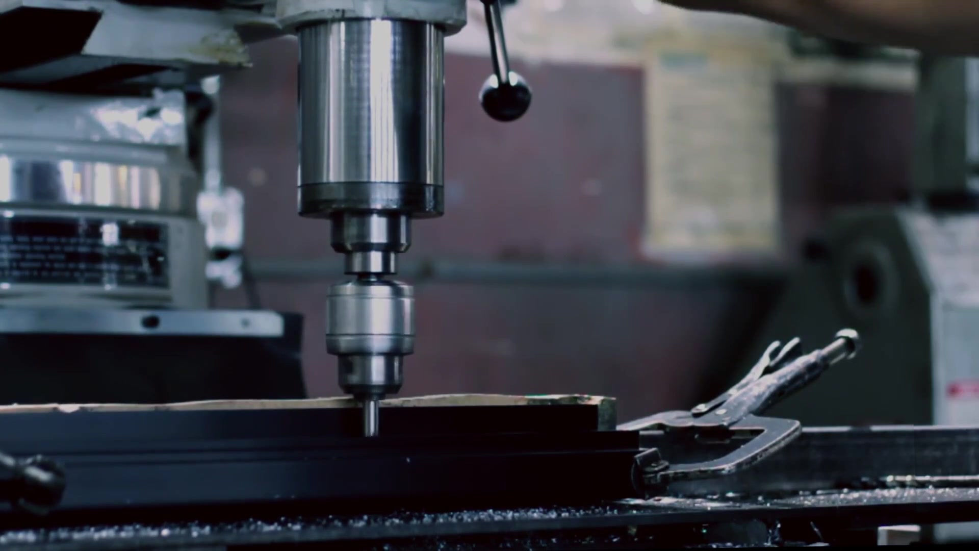
Mesomanufacturing - Mesoscale Manufacturing - Miniature Device Fabrication - Tiny Motors - AGS-TECH Inc. - New Mexico Mesoscale Manufacturing / Mesomanufacturing With conventional production techniques we produce “macroscale” structures that are relatively large and visible to the naked eye. With MESOMANUFACTURING however we produce components for miniature devices. Mesomanufacturing is also referred to as MESOSCALE MANUFACTURING or MESO-MACHINING. Mesomanufacturing overlaps both macro and micromanufacturing. Examples of mesomanufacturing are hearing aides, stents, very small motors. The first approach in mesomanufacturing is to scale macromanufacturing processes down. For example a tiny lathe with dimensions in the few dozen millimeters and a motor of 1.5W weighing 100 grams is a good example of mesomanufacturing where downscaling has taken place. The second approach is to scale micromanufacturing processes up. As an example LIGA processes can be upscaled and enter the realm of mesomanufacturing. Our mesomanufacturing processes are bridging the gap between silicon-based MEMS processes and conventional miniature machining. Mesoscale processes can fabricate two and three-dimensional parts having micron size features in traditional materials such as stainless steels, ceramics, and glass. Mesomanufacturing processes that are currently available to us include, focused ion beam (FIB) sputtering, micro-milling, micro-turning, excimer laser ablation, femto-second laser ablation, and micro electro-discharge (EDM) machining. These mesoscale processes employ subtractive machining technologies (i.e., material removal), whereas the LIGA process, is an additive mesoscale process. Mesomanufacturing processes have different capabilities and performance specifications. Machining performance specifications of interest include minimum feature size, feature tolerance, feature location accuracy, surface finish, and material removal rate (MRR). We have the capability of mesomanufacturing electro-mechanical components that require mesoscale parts. The mesoscale parts fabricated by subtractive mesomanufacturing processes have unique tribological properties because of the variety of materials and the surface conditions produced by the different mesomanufacturing processes. These subtractive mesoscale machining technologies bring us concerns related to cleanliness, assembly, and tribology. Cleanliness is vital in mesomanufacturing because mesoscale dirt and debris particle size created during the meso-machining process can be comparable to mesoscale features. Mesoscale milling and turning can create chips and burrs that can block holes. Surface morphology and surface finish conditions vary greatly depending on the mesomanufacturing method. Mesoscale parts are difficult to handle and align which makes assembly a challenge which most of our competitors are unable to overcome. Our yield rates in mesomanufacturing is far higher than our competitors which gives us the advantage of being able to offer better prices. MESOSCALE MACHINING PROCESSES: Our major mesomanufacturing techniques are Focused Ion Beam (FIB), Micro-milling, & Micro-turning, laser meso-machining, Micro-EDM (electro-discharge machining) Mesomanufacturing using focused Ion Beam (FIB), Micro-milling, & Micro-turning: The FIB sputters material from a workpiece by Gallium ion beam bombardment. The workpiece is mounted to a set of precision stages and is placed in a vacuum chamber underneath the source of Gallium. The translation and rotation stages in the vacuum chamber make various locations on the work piece available to the beam of Gallium ions for FIB mesomanufacturing. A tunable electric field scans the beam to cover a pre-defined projected area. A high voltage potential causes a source of Gallium ions to accelerate and collide with the work piece. The collisions strip away atoms from the work piece. The result of the FIB meso-machining process can be the creation of a near vertical facets. Some FIBs available to us have beam diameters as small as 5 nanometers, making the FIB a mesoscale and even microscale capable machine. We mount micro-milling tools on high precision milling machines to machine channels in aluminum. Using FIB we can fabricate micro-turning tools which can then be used on a lathe to fabricate finely threaded rods. In other words, FIB can be used to machine hard tooling besides directly meso-machining features onto the end work piece. The slow material removal rate has rendered the FIB as impractical for directly machining large features. The hard tools, however, can remove material at an impressive rate and are durable enough for several hours of machining time. Nevertheless, the FIB is practical for directly meso-machining complex three dimensional shapes that do not require a substantial material removal rate. Length of exposure and angle of incidence can greatly affect the geometry of directly machined features. Laser Mesomanufacturing: Excimer lasers are used for mesomanufacturing. The excimer laser machines material by pulsing it with nanosecond pulses of ultraviolet light. The work piece is mounted to precision translational stages. A controller coordinates the motion of the work piece relative to the stationary UV laser beam and coordinates the firing of the pulses. A mask projection technique can be used to define meso-machining geometries. The mask is inserted into the expanded part of the beam where the laser fluence is too low to ablate the mask. The mask geometry is de-magnified through the lens and projected onto the work piece. This approach can be used for machining multiple holes (arrays) simultaneously. Our excimer and YAG lasers can be used to machine polymers, ceramics, glass and metals having feature sizes as small as 12 microns. Good coupling between the UV wavelength (248 nm) and the workpiece in laser mesomanufacturing / meso-machining results in vertical channel walls. A cleaner laser meso-machining approach is to use a Ti-sapphire femtosecond laser. The detectable debris from such mesomanufacturing processes are nano-sized particles. Deep one micron-size features can be microfabricated using the femtosecond laser. The femtosecond laser ablation process is unique in that it breaks atomic bonds instead of thermally ablating material. The femtosecond laser meso-machining / micromachining process has a special place in mesomanufacturing because it is cleaner, micron capable, and it is not material specific. Mesomanufacturing using Micro-EDM (electro-discharge machining): Electro-discharge machining removes material through a spark erosion process. Our micro-EDM machines can produce features as small as 25 microns. For the sinker and the wire micro-EDM machine, the two major considerations for determining feature size are the electrode size and the over-bum gap. Electrodes little over 10 microns in diameter and over-bum as little as a few microns are being used. Creating an electrode having a complex geometry for the sinker EDM machine requires know-how. Both graphite and copper are popular as electrode materials. One approach to fabricating a complicated sinker EDM electrode for a mesoscale part is to use the LIGA process. Copper, as the electrode material, can be plated into LIGA molds. The copper LIGA electrode can then be mounted onto the sinker EDM machine for mesomanufacturing a part in a different material such as stainless steel or kovar. No one mesomanufacturing process is sufficient for all operations. Some mesoscale processes are more wide reaching than others, but each process has its niche. Most of the time we require a variety of materials to optimize performance of mechanical components and are comfortable with traditional materials such as stainless steel because these materials have a long history and have been very well characterized through the years. Mesomanufacturing processes allow us to use traditional materials. Subtractive mesoscale machining technologies expand our material base. Galling may be an-issue with some material combinations in mesomanufacturing. Each particular mesoscale machining process uniquely affects the surface roughness and morphology. Micro-milling and micro-turning may generate burrs and particles that can cause mechanical problems. Micro-EDM may leave a recast layer that can have particular wear and friction characteristics. Friction effects between mesoscale parts may have limited points of contact and are not accurately modeled by surface contact models. Some mesoscale machining technologies, such as micro-EDM, are fairly mature, as opposed to others, such as femtosecond laser meso-machining, which still require additional development. CLICK Product Finder-Locator Service PREVIOUS PAGE
- Micro-Optics - Micro-Optical - Microoptical - Wafer Level Optics
Micro-Optics, Micro-Optical, Microoptical, Wafer Level Optics, Gratings, Fresnel Lenses, Lens Array, Micromirrors, Micro Reflectors, Collimators, Aspheres, LED Micro-Optics Manufacturing One of the fields in microfabrication we are involved in is MICRO-OPTICS MANUFACTURING. Micro-optics allows the manipulation of light and the management of photons with micron and sub-micron scale structures and components. Some applications of MICRO-OPTICAL COMPONENTS and SUBSYSTEMS are: Information technology: In micro-displays, micro-projectors, optical data storage, micro-cameras, scanners, printers, copiers…etc. Biomedicine: Minimally-invasive/point of care diagnostics, treatment monitoring, micro-imaging sensors, retinal implants, micro-endoscopes. Lighting: Systems based on LEDs and other efficient light sources Safety and Security Systems: Infrared night vision systems for automotive applications, optical fingerprint sensors, retinal scanners. Optical Communication & Telecommunication: In photonic switches, passive fiber optic components, optical amplifiers, mainframe and personal computer interconnect systems Smart structures: In optical fiber-based sensing systems and much more The types of micro-optical components and subsystems we manufacture and supply are: - Wafer Level Optics - Refractive Optics - Diffractive Optics - Filters - Gratings - Computer Generated Holograms - Hybrid Microoptical Components - Infrared Micro-Optics - Polymer Micro-Optics - Optical MEMS - Monolithically and Discretely Integrated Micro-Optic Systems Some of our most widely used micro-optical products are: - Bi-convex and plano-convex lenses - Achromat lenses - Ball lenses - Vortex Lenses - Fresnel Lenses - Multifocal Lens - Cylindrical Lenses - Graded Index (GRIN) Lenses - Micro-Optical Prisms - Aspheres - Arrays of Aspheres - Collimators - Micro-Lens Arrays - Diffraction Gratings - Wire-Grid Polarizers - Micro-Optic Digital Filters - Pulse Compression Gratings - LED Modules - Beam Shapers - Beam Sampler - Ring Generator - Micro-Optical Homogenizers / Diffusers - Multispot Beam Splitters - Dual Wavelength Beam Combiners - Micro-Optical Interconnects - Intelligent Micro-Optics Systems - Imaging Microlenses - Micromirrors - Micro Reflectors - Micro-Optical Windows - Dielectric Mask - Iris Diaphragms Let us provide you some basic information about these micro-optical products and their applications: BALL LENSES: Ball lenses are completely spherical micro-optic lenses most commonly used to couple light in and out of fibers. We supply a range of micro-optic stock ball lenses and can manufacture also to your own specifications. Our stock ball lenses from quartz have excellent UV and IR transmission between 185nm to >2000nm, and our sapphire lenses have a higher refractive index, allowing a very short focal length for excellent fiber coupling. Micro-optical ball lenses from other materials and diameters are available. Besides fiber coupling applications, micro-optical ball lenses are used as objective lenses in endoscopy, laser measurement systems and bar-code scanning. On the other hand, micro-optic half ball lenses offer uniform dispersion of light and are widely used in LED displays and traffic lights. MICRO-OPTICAL ASPHERES and ARRAYS: Aspheric surfaces have a non-spherical profile. Use of aspheres can reduce the number of optics required to reach a desired optical performance. Popular applications for micro-optical lens arrays with spherical or aspherical curvature are imaging and illumination and the effective collimation of laser light. Substitution of a single aspheric microlens array for a complex multilens system results not only in smaller size, lighter weight, compact geometry, and lower cost of an optical system, but also in significant improvement of its optical performance such as better imaging quality. However, the fabrication of aspheric microlenses and microlens arrays is challenging, because conventional technologies used for macro-sized aspheres like single-point diamond milling and thermal reflow are not capable of defining a complicated micro-optic lens profile in an area as small as several to tens of micrometers. We possess the know-how of producing such micro-optical structures using advanced techniques such as femtosecond lasers. MICRO-OPTICAL ACHROMAT LENSES: These lenses are ideal for applications requiring color correction, while aspheric lenses are designed to correct spherical aberration. An achromatic lens or achromat is a lens that is designed to limit the effects of chromatic and spherical aberration. Micro-optical achromatic lenses make corrections to bring two wavelengths (such as red and blue colors) into focus on the same plane. CYLINDRICAL LENSES: These lenses focus light into a line instead of a point, as a spherical lens would. The curved face or faces of a cylindrical lens are sections of a cylinder, and focus the image passing through it into a line parallel to the intersection of the surface of the lens and a plane tangent to it. The cylindrical lens compresses the image in the direction perpendicular to this line, and leaves it unaltered in the direction parallel to it (in the tangent plane). Tiny micro-optical versions are available which are suitable for use in micro optical environments, requiring compact-size fiber optical components, laser systems, and micro-optical devices. MICRO-OPTICAL WINDOWS and FLATS: Milimetric micro-optical windows meeting tight tolerance requirements are available. We can custom manufacture them to your specifications from any of the optical grade glasses. We offer a variety of micro-optical windows made of different materials such as fused silica, BK7, sapphire, zinc sulphide….etc. with transmission from UV to middle IR range. IMAGING MICROLENSES: Microlenses are small lenses, generally with a diameter less than a millimetre (mm) and as small as 10 micrometres. Imaging Lenses are used to view objects in imaging systems. Imaging Lenses are used in imaging systems to focus an image of an examined object onto a camera sensor. Depending on the lens, imaging lenses can be used to remove parallax or perspective error. They can also offer adjustable magnifications, field of views, and focal lengths. These lenses allow an object to be viewed in several ways to illustrate certain features or characteristics that may be desirable in certain applications. MICROMIRRORS: Micromirror devices are based on microscopically small mirrors. The mirrors are Microelectromechanical systems (MEMS). The states of these micro-optical devices are controlled by applying a voltage between the two electrodes around the mirror arrays. Digital micromirror devices are used in video projectors and optics and micromirror devices are used for light deflection and control. MICRO-OPTIC COLLIMATORS & COLLIMATOR ARRAYS: A variety of micro-optical collimators are available off-the-shelf. Micro-optical small beam collimators for demanding applications are produced using laser fusion technology. The fiber end is directly fused to the optical center of the lens, thereby eliminated epoxy within the optical path. The micro-optic collimator lens surface is then laser polished to within a millionth of an inch of the ideal shape. Small Beam collimators produce collimated beams with beam waists under a millimeter. Micro-optical small beam collimators are typically used at 1064, 1310 or 1550 nm wavelengths. GRIN lens based micro-optic collimators are also available as well as collimator array and collimator fiber array assemblies. MICRO-OPTICAL FRESNEL LENSES: A Fresnel lens is a type of compact lens designed to allow the construction of lenses of large aperture and short focal length without the mass and volume of material that would be required by a lens of conventional design. A Fresnel lens can be made much thinner than a comparable conventional lens, sometimes taking the form of a flat sheet. A Fresnel lens can capture more oblique light from a light source, thus allowing the light to be visible over greater distances. The Fresnel lens reduces the amount of material required compared to a conventional lens by dividing the lens into a set of concentric annular sections. In each section, the overall thickness is decreased compared to an equivalent simple lens. This can be viewed as dividing the continuous surface of a standard lens into a set of surfaces of the same curvature, with stepwise discontinuities between them. Micro-optic Fresnel lenses focus light by refraction in a set of concentric curved surfaces. These lenses can be made very thin and lightweight. Micro-optical Fresnel lenses offer opportunities in optics for highresolution Xray applications, throughwafer optical interconnection capabilities. We have a number of fabrication methods including micromolding and micromachining to manufacture micro-optical Fresnel lenses and arrays specifically for your applications. We can design a positive Fresnel lens as a collimator, collector or with two finite conjugates. Micro-Optical Fresnel lenses are usually corrected for spherical aberrations. Micro-optic positive lenses can be metalized for use as a second surface reflector and negative lenses can be metalized for use as a first surface reflector. MICRO-OPTICAL PRISMS: Our line of precision micro-optics includes standard coated and uncoated micro prisms. They are suitable for use with laser sources and imaging applications. Our micro-optical prisms have submilimeter dimensions. Our coated micro-optical prisms can also be used as mirror reflectors with respect to incoming light. Uncoated prisms act as mirrors for light incident on one of the short sides since incident light is totally internally reflected at the hypotenuse. Examples of our micro-optical prism capabilities include right angle prisms, beamsplitter cube assemblies, Amici prisms, K-prisms, Dove prisms, Roof prisms, Cornercubes, Pentaprisms, Rhomboid prisms, Bauernfeind prisms, Dispersing prisms, Reflecting prisms. We also offer light guiding and de-glaring optical micro-prisms made from acrylic, polycarbonate and other plastic materials by hot embossing manufacturing process for applications in lamps and luminaries, LEDs. They are highly efficient, strong light guiding precise prism surfaces, support luminaries to fulfill office regulations for de-glaring. Additional customized prism structures are possible. Microprisms and microprism arrays on wafer level are also possible using microfabrication techniques. DIFFRACTION GRATINGS: We offer design and manufacture of diffractive micro-optical elements (DOEs). A diffraction grating is an optical component with a periodic structure, which splits and diffracts light into several beams travelling in different directions. The directions of these beams depend on the spacing of the grating and the wavelength of the light so that the grating acts as the dispersive element. This makes grating a suitable element to be used in monochromators and spectrometers. Using wafer-based lithography, we produce diffractive micro-optical elements with exceptional thermal, mechanical and optical performance characteristics. Wafer-level processing of micro-optics provides excellent manufacturing repeatability and economic output. Some of the available materials for diffractive micro-optical elements are crystal-quartz, fused-silica, glass, silicon and synthetic substrates. Diffraction gratings are useful in applications such as spectral analysis / spectroscopy, MUX/DEMUX/DWDM, precision motion control such as in optical encoders. Lithography techniques make the fabrication of precision micro-optical gratings with tightly-controlled groove spacings possible. AGS-TECH offers both custom and stock designs. VORTEX LENSES: In laser applications there is a need to convert a Gaussian beam to a donut-shaped energy ring. This is achieved using Vortex lenses. Some applications are in lithography and high-resolution microscopy. Polymer on glass Vortex phase plates are also available. MICRO-OPTICAL HOMOGENIZERS / DIFFUSERS: A variety of technologies are used to fabricate our micro-optical homogenizers and diffusers, including embossing, engineered diffuser films, etched diffusers, HiLAM diffusers. Laser Speckle is the optical phenomena resulting from the random interference of coherent light. This phenomenon is utilized to measure the Modulation Transfer Function (MTF) of detector arrays. Microlens diffusers are shown to be efficient micro-optic devices for speckle generation. BEAM SHAPERS: A micro-optic beam shaper is an optic or a set of optics that transforms both the intensity distribution and the spatial shape of a laser beam to something more desirable for a given application. Frequently, a Gaussian-like or non-uniform laser beam is transformed to a flat top beam. Beam shaper micro-optics are used to shape and manipulate single mode and multi-mode laser beams. Our beam shaper micro-optics provide circular, square, rectilinear, hexagonal or line shapes, and homogenize the beam (flat top) or provide a custom intensity pattern according to the requirements of the application. Refractive, diffractive and reflective micro-optical elements for laser beam shaping and homogenizing have been manufactured. Multifunctional micro-optical elements are used for shaping arbitrary laser beam profiles into a variety of geometries like, a homogeneous spot array or line pattern, a laser light sheet or flat-top intensity profiles. Fine beam application examples are cutting and keyhole welding. Broad beam application examples are conduction welding, brazing, soldering, heat treatment, thin film ablation, laser peening. PULSE COMPRESSION GRATINGS: Pulse compression is a useful technique that takes advantage of the relationship between pulse duration and spectral width of a pulse. This enables the amplification of laser pulses above the normal damage threshold limits imposed by the optical components in the laser system. There are linear and nonlinear techniques for reducing the durations of optical pulses. There is variety of methods for temporally compressing / shortening optical pulses, i.e., reducing the pulse duration. These methods generally start in the picosecond or femtosecond region, i.e. already in the regime of ultrashort pulses. MULTISPOT BEAM SPLITTERS: Beam splitting by means of diffractive elements is desirable when one element is required to produce several beams or when very exact optical power separation is required. Precise positioning can also be achieved, for example, to create holes at clearly defined and accurate distances. We have Multi-Spot Elements, Beam Sampler Elements, Multi-Focus Element. Using a diffractive element, collimated incident beams are split into several beams. These optical beams have equal intensity and equal angle to one another. We have both one-dimensional and two-dimensional elements. 1D elements split beams along a straight line whereas 2D elements produce beams arranged in a matrix of, for example, 2 x 2 or 3 x 3 spots and elements with spots that are arranged hexagonally. Micro-optical versions are available. BEAM SAMPLER ELEMENTS: These elements are gratings that are used for inline monitoring of high power lasers. The ± first diffraction order can be used for beam measurements. Their intensity is significantly lower than that of the main beam and can be custom designed. Higher diffraction orders can also be used for measurement with even lower intensity. Variations in intensity and changes in the beam profile of high power lasers can be reliably monitored inline using this method. MULTI-FOCUS ELEMENTS: With this diffractive element several focal points can be created along the optical axis. These optical elements are used in sensors, ophthalmology, material processing. Micro-optical versions are available. MICRO-OPTICAL INTERCONNECTS: Optical interconnects have been replacing electrical copper wires at the different levels in the interconnect hierarchy. One of the possibilities to bring the advantages of micro-optics telecommunications to the computer backplane, the printed circuit board, the inter-chip and on-chip interconnect level, is to use free-space micro-optical interconnect modules made of plastic. These modules are capable of carrying high aggregate communication bandwidth through thousands of point-to-point optical links on a footprint of a square centimeter. Contact us for off-shelf as well as custom tailored micro-optical interconnects for computer backplane, the printed circuit board, the inter-chip and on-chip interconnect levels. INTELLIGENT MICRO-OPTICS SYSTEMS: Intelligent micro-optic light modules are used in smart phones and smart devices for LED flash applications, in optical interconnects for transporting data in supercomputers and telecommunications equipment, as miniaturized solutions for near-infrared beam shaping, detection in gaming applications and for supporting gesture control in natural user interfaces. Sensing opto-electronic modules are used for a number of product applications such as ambient light and proximity sensors in smart phones. Intelligent imaging micro-optic systems are used for primary and front-facing cameras. We offer also customized intelligent micro-optical systems with high performance and manufacturability. LED MODULES: You can find our LED chips, dies and modules on our page Lighting & Illumination Components Manufacturing by clicking here. WIRE-GRID POLARIZERS: These consist of a regular array of fine parallel metallic wires, placed in a plane perpendicular to the incident beam. The polarization direction is perpendicular to the wires. Patterned polarizers have applications in polarimetry, interferometry, 3D displays, and optical data storage. Wire-grid polarizers are extensively used in infrared applications. On the other hand micropatterned wire-grid polarizers have limited spatial resolution and poor performance at visible wavelengths, are susceptible to defects and cannot be easily extended to non-linear polarizations. Pixelated polarizers use an array of micro-patterned nanowire grids. The pixelated micro-optical polarizers can be aligned with cameras, plane arrays, interferometers, and microbolometers without the need for mechanical polarizer switches. Vibrant images distinguishing between multiple polarizations across the visible and IR wavelengths can be captured simultaneously in real-time enabling fast, high resolution images. Pixelated micro-optical polarizers also enable clear 2D and 3D images even in low-light conditions. We offer patterned polarizers for two, three and four-state imaging devices. Micro-optical versions are available. GRADED INDEX (GRIN) LENSES: Gradual variation of the refractive index (n) of a material can be used to produce lenses with flat surfaces, or lenses that do not have the aberrations typically observed with traditional spherical lenses. Gradient-index (GRIN) lenses may have a refraction gradient that is spherical, axial, or radial. Very small micro-optical versions are available. MICRO-OPTIC DIGITAL FILTERS: Digital neutral density filters are used to control the intensity profiles of illumination and projection systems. These micro-optic filters contain well-defined metal absorber micro-structures that are randomly distributed on a fused silica substrate. Properties of these micro-optical components are high accuracy, large clear aperture, high damage threshold, broadband attenuation for DUV to IR wavelengths, well defined one or two dimensional transmission profiles. Some applications are soft edge apertures, precise correction of intensity profiles in illumination or projection systems, variable attenuation filters for high-power lamps and expanded laser beams. We can customize the density and size of the structures to meet precisely the transmission profiles required by the application. MULTI-WAVELENGTH BEAM COMBINERS: Multi-Wavelength beam combiners combine two LED collimators of different wavelengths into a single collimated beam. Multiple combiners can be cascaded to combine more than two LED collimator sources. Beam combiners are made of high-performance dichroic beam splitters that combine two wavelengths with >95% efficiency. Very small micro-optic versions are available. CLICK Product Finder-Locator Service PREVIOUS PAGE
- Plasma Machining, HF Plasma Cutting, Plasma Gouging, CNC, Arc Welding
Plasma Machining - HF Plasma Cutting - Plasma Gouging - CNC - Plasma Arc Welding - PAW - GTAW - AGS-TECH Inc. - New Mexico Plasma Machining & Cutting We use the PLASMA CUTTING and PLASMA MACHINING processes to cut and machine steel, aluminum, metals and other materials of different thicknesses using a plasma torch. In plasma-cutting (also sometimes called PLASMA-ARC CUTTING), an inert gas or compressed air is blown at high speed out of a nozzle and simultaneously an electrical arc is formed through that gas from the nozzle to the surface being cut, turning a portion of that gas to plasma. To simplify, plasma can be described as the fourth state of matter. The three states of matter are solid, liquid and gas. For a common example, water, these three states are ice, water and steam. The difference between these states relates to their energy levels. When we add energy in the form of heat to ice, it melts and forms water. When we add more energy, the water vaporizes in the form of steam. By adding more energy to steam these gases become ionized. This ionization process causes the gas to become electrically conductive. We call this electrically conductive, ionized gas a “plasma”. The plasma is very hot and melts the metal being cut and at the same time blowing the molten metal away from the cut. We use plasma for cutting thin and thick, ferrous and nonferrous materials alike. Our hand-held torches can usually cut up to 2 inches thick steel plate, and our stronger computer-controlled torches can cut steel up to 6 inches thick. Plasma cutters produce a very hot and localized cone to cut with, and are therefore very suitable for cutting metal sheets in curved and angled shapes. The temperatures generated in plasma-arc cutting are very high and around 9673 Kelvin in the oxygen plasma torch. This offers us a fast process, small kerf width, and good surface finish. In our systems using tungsten electrodes, the plasma is inert, formed using either argon, argon-H2 or nitrogen gases. However, we also use sometimes oxidizing gases, such as air or oxygen, and in those systems the electrode is copper with hafnium. The advantage of an air plasma torch is that it uses air instead of expensive gases, thus potentially reducing overall cost of machining . Our HF-TYPE PLASMA CUTTING machines use a high-frequency, high-voltage spark to ionize the air through the torch head and initiate arcs. Our HF plasma cutters do not require the torch to be in contact with the workpiece material at the start, and are suitable for applications involving COMPUTER NUMERICAL CONTROL (CNC) cutting. Other manufacturers are using primitive machines that require tip contact with the parent metal to start and then the gap separation occurs. These more primitive plasma cutters are more susceptible to contact tip and shield damage at starting. Our PILOT-ARC TYPE PLASMA machines use a two step process for producing plasma, without the need for initial contact. In the first step, a high-voltage, low current circuit is used to initialize a very small high-intensity spark within the torch body, generating a small pocket of plasma gas. This is called the pilot arc. The pilot arc has a return electrical path built into the torch head. The pilot arc is maintained and preserved until it is brought into proximity of the workpiece. There the pilot arc ignites the main plasma cutting arc. Plasma arcs are extremely hot and are in the range of 25,000 °C = 45,000 °F. A more traditional method we also deploy is OXYFUEL-GAS CUTTING (OFC) where we use a torch as in welding. The operation is used in cutting of steel, cast iron and cast steel. The principle of cutting in oxyfuel-gas cutting is based on oxidation, burning and melting of the steel. Kerf widths in oxyfuel-gas cutting are in the neighborhood of 1.5 to 10mm. The plasma arc process has been seen as an alternative to the oxy-fuel process. The plasma-arc process differs from the oxy-fuel process in that it operates by using the arc to melt the metal whereas in the oxy-fuel process, the oxygen oxidizes the metal and the heat from the exothermic reaction melts the metal. Therefore, unlike the oxy-fuel process, the plasma-process can be applied for cutting metals which form refractory oxides such as stainless steel, aluminium, and non-ferrous alloys. PLASMA GOUGING a similar process to plasma cutting, is typically performed with the same equipment as plasma cutting. Instead of cutting the material, plasma gouging uses a different torch configuration. The torch nozzle and gas diffuser is usually different, and a longer torch-to-workpiece distance is maintained for blowing away metal. Plasma gouging can be used in various applications, including removing a weld for rework. Some of our plasma cutters are built in to the CNC table. CNC tables have a computer to control the torch head to produce clean sharp cuts. Our modern CNC plasma equipment is capable of multi-axis cutting of thick materials and allowing opportunities for complex welding seams that are not possible otherwise. Our plasma-arc cutters are highly automated through the use of programmable controls. For thinner materials, we prefer laser cutting to plasma cutting, mostly because of our laser cutter's superior hole-cutting abilities. We also deploy vertical CNC plasma cutting machines, offering us a smaller footprint, increased flexibility, better safety and faster operation. The quality of the plasma cut edge is similar to that achieved with the oxy-fuel cutting processes. However, because the plasma process cuts by melting, a characteristic feature is the greater degree of melting towards the top of the metal resulting in top edge rounding, poor edge squareness or a bevel on the cut edge. We use new models of plasma torches with a smaller nozzle and a thinner plasma arc to improve arc constriction to produce more uniform heating at the top and bottom of the cut. This allows us to obtain near-laser precision on plasma cut and machined edges. Our HIGH TOLERANCE PLASMA ARC CUTTING (HTPAC) systems operate with a highly constricted plasma. Focusing of the plasma is achieved by forcing the oxygen generated plasma to swirl as it enters the plasma orifice and a secondary flow of gas is injected downstream of the plasma nozzle. We have a separate magnetic field surrounding the arc. This stabilises the plasma jet by maintaining the rotation induced by the swirling gas. By combining precision CNC control with these smaller and thinner torches we are capable to produce parts that require little or no finishing. Material removal rates in plasma-machining are much higher than in the Electric-Discharge-Machining (EDM) and Laser-Beam-Machining (LBM) processes, and parts can be machined with good reproducibility. PLASMA ARC WELDING (PAW) is a process similar to gas tungsten arc welding (GTAW). The electric arc is formed between an electrode generally made of sintered tungsten and the workpiece. The key difference from GTAW is that in PAW, by positioning the electrode within the body of the torch, the plasma arc can be separated from the shielding gas envelope. The plasma is then forced through a fine-bore copper nozzle which constricts the arc and the plasma exiting the orifice at high velocities and temperatures approaching 20,000 °C. Plasma arc welding is an advancement over the GTAW process. The PAW welding process uses a non-consumable tungsten electrode and an arc constricted through a fine-bore copper nozzle. PAW can be used to join all metals and alloys that are weldable with GTAW. Several basic PAW process variations are possible by varying the current, plasma gas flow rate, and the orifice diameter, including: Micro-plasma (< 15 Amperes) Melt-in mode (15–400 Amperes) Keyhole mode (>100 Amperes) In plasma arc welding (PAW) we obtain a greater energy concentration as compared to GTAW. Deep and narrow penetration is achievable, with a maximum depth of 12 to 18 mm (0.47 to 0.71 in) depending on the material. Greater arc stability allows a much longer arc length (stand-off), and much greater tolerance to arc length changes. As a disadvantage however, PAW requires relatively expensive and complex equipment as compared to GTAW. Also the torch maintenance is critical and more challenging. Other disadvantages of PAW are: Welding procedures tend to be more complex and less tolerant to variations in fit-up, etc. Operator skill required is a little more than for GTAW. Orifice replacement is necessary. CLICK Product Finder-Locator Service PREVIOUS PAGE
- Camera Systems & Components, Optic Scanner, Optical Readers, CCD
Camera Systems - Components - Optic Scanner - Optical Readers - Imaging System - CCD - Optomechanical Systems - IR Cameras Customized Camera Systems Manufacturing & Assembly AGS-TECH offers: • Camera systems, camera components and custom camera assemblies • Custom designed and manufactured optical scanners, readers, optical security product assemblies. • Precision optical, opto-mechanical and electro-optical assemblies integrating imaging and nonimaging optics, LED lighting, fiber optics and CCD cameras • Among the products our optical engineers have developed are: - Omni-directional periscope and camera for surveillance and security applications. 360 x 60º field of view high resolution image, no stitching required. - Inner cavity wide angle video camera - Super slim 0.6 mm diameter flexible video endoscope. All medical video couplers fit over standard endoscope eyepieces and are completely sealed and soakable. For our medical endoscope and camera systems, please visit: http://www.agsmedical.com - Video camera and coupler for semi-rigid endoscope - Eye-Q Videoprobe. Non-contact zoom videoprobe for coordinate measuring machines. - Optical spectrograph & IR imaging system (OSIRIS) for ODIN satellite. Our engineers worked on the flight unit assembly, alignment, integration and test. - Wind imaging interferometer (WINDII) for NASA upper atmosphere research satellite (UARS). Our engineers worked on consulting on assembly, integration and test. WINDII performance and operational lifetime far exceeded the design goals and requirements. Depending on your application, we will determine what dimensions, pixel count, resolution, wavelength sensitivity your camera application requires. We can build systems for you suitable for infrared, visible and other wavelengths. Contact us today to find out more. Dowload brochure for our DESIGN PARTNERSHIP PROGRAM Developing a customized camera system can take relatively longer lead times and cost more as compared to ready-to-use systems. Therefore please click on the blue links below to check whether any of our ready-to-use products fit your application: Barcode and Fixed Mount Scanners - RFID Products - Mobile Computers - Micro Kiosks OEM Technology (We private label these with your brand name and logo if you wish) Barcode Scanners (We private label these with your brand name and logo if you wish) Fixed Industrial Scanners (We private label these with your brand name and logo if you wish) Hikrobot Machine Vision Products Hikrobot Smart Machine Vision Products Hikrobot Machine Vision Standard Products Hikvision Logistic Vision Solutions Private Label Medical Endoscopes and Visualization Systems (We can put your company name and logo on these) Also make sure to download our comprehensive electric & electronic components catalog for off-shelf products by CLICKING HERE. CLICK Product Finder-Locator Service PREVIOUS PAGE
- Surface Treatment and Modification - Surface Engineering - Hardening
Surface Treatment and Modification - Surface Engineering - Hardening - Plasma - Laser - Ion Implantation - Electron Beam Processing at AGS-TECH Surface Treatments and Modification Surfaces cover everything. The appeal and functions material surfaces provide us are of utmost importance. Therefore SURFACE TREATMENT and SURFACE MODIFICATION are among our everyday industrial operations. Surface treatment & modification leads to enhanced surface properties and can be performed either as a final finishing operation or prior to a coating or joining operation. The processes of surface treatments and modification (also referred to as SURFACE ENGINEERING), tailor the surfaces of materials and products to: - Control friction and wear - Improve corrosion resistance - Enhance adhesion of subsequent coatings or joined parts - Change physical properties conductivity, resistivity, surface energy and reflection - Change chemical properties of surfaces by introducing functional groups - Change dimensions - Change the appearance, e.g., color, roughness…etc. - Clean and / or disinfect the surfaces Using surface treatment and modification, the functions and service lives of materials can be improved. Our common surface treatment and modification methods can be divided into two major categories: Surface Treatment and Modification That Covers Surfaces: Organic Coatings: The organic coatings apply paints, cements, laminates, fused powders and lubricants on the surfaces of materials. Inorganic Coatings: Our popular inorganic coatings are electroplating, autocatalytic plating (electroless platings), conversion coatings, thermal sprays, hot dipping, hardfacing, furnace fusing, thin film coatings such as SiO2, SiN on metal, glass, ceramics,….etc. Surface treatment and modification involving coatings is explained in detail under the related submenu, please click here Functional Coatings / Decorative Coatings / Thin Film / Thick Film Surface Treatment and Modification That Alters Surfaces: Here on this page we will concentrate on these. Not all of the surface treatment and modification techniques we describe below are on the micro or nano-scale, but we will nevertheless mention about them briefly since the basic objectives and methods are similar to significant extent to those that are on the micromanufacturing scale. Hardening: Selective surface hardening by laser, flame, induction and electron beam. High Energy Treatments: Some of our high energy treatments include ion implantation, laser glazing & fusion, and electron beam treatment. Thin Diffusion Treatments: Thin diffusion processes include ferritic-nitrocarburizing, boronizing, other high temperature reaction processes such as TiC, VC. Heavy Diffusion Treatments: Our heavy diffusion processes include carburizing, nitriding, and carbonitriding. Special Surface Treatments: Special treatments such as cryogenic, magnetic, and sonic treatments affect both the surfaces and the bulk materials. The selective hardening processes can be carried out by flame, induction, electron beam, laser beam. Large substrates are deep hardened using flame hardening. Induction hardening on the other hand is used for small parts. Laser and electron beam hardening are sometimes not distinguished from those in hardfacings or high-energy treatments. These surface treatment and modification processes are applicable only to steels that have sufficient carbon and alloy content to allow quench hardening. Cast irons, carbon steels, tool steels, and alloy steels are suitable for this surface treatment and modification method. Dimensions of parts are not significantly altered by these hardening surface treatments. Depth of hardening can vary from 250 microns to the whole section depth. However, in the whole section case, the section must be thin, less than 25 mm (1 in), or small, since the hardening processes require a rapid cooling of materials, sometimes within a second. This is difficult to achieve in large workpieces, and therefore in large sections, only the surfaces can be hardened. As a popular surface treatment and modification process we harden springs, knife blades, and surgical blades among many other products. High-energy processes are relatively new surface treatment and modification methods. Properties of surfaces are changed without changing the dimensions. Our popular high-energy surface treatment processes are electron beam treatment, ion implantation, and laser beam treatment. Electron Beam Treatment: Electron beam surface treatment alters the surface properties by rapid heating and rapid cooling — in the order of 10Exp6 Centigrade/sec (10exp6 Fahrenheit/sec) in a very shallow region around 100 microns near the material surface. Electron beam treatment can also be used in hardfacing to produce surface alloys. Ion Implantation: This surface treatment and modification method uses electron beam or plasma to convert gas atoms to ions with sufficient energy, and implant/insert the ions into atomic lattice of the substrate, accelerated by magnetic coils in a vacuum chamber. Vacuum makes it easier for ions to move freely in the chamber. The mismatch between implanted ions and the surface of the metal creates atomic defects that hardens the surface. Laser Beam Treatment: Like the electron beam surface treatment and modification, laser beam treatment alters the surface properties by rapid heating and rapid cooling in a very shallow region near the surface. This surface treatment & modification method can also be used in hardfacing to produce surface alloys. A know-how in Implant dosages and treatment parameters makes it possible for us to use these high energy surface treatment techniques in our fabrication plants. Thin Diffusion Surface Treatments: Ferritic nitrocarburizing is a case hardening process that diffuses nitrogen and carbon into ferrous metals at sub-critical temperatures. The processing temperature is usually at 565 Centigrade (1049 Fahrenheit). At this temperature steels and other ferrous alloys are still in a ferritic phase, which is advantageous compared to other case hardening processes that occur in the austenitic phase. The process is used to improve: •scuffing resistance •fatigue properties •corrosion resistance Very little shape distortion occurs during the hardening process thanks to the low processing temperatures. Boronizing, is the process where boron is introduced to a metal or alloy. It is a surface hardening and modification process by which boron atoms are diffused into the surface of a metal component. As a result the surface contains metal borides, such as iron borides and nickel borides. In their pure state these borides have extremely high hardness and wear resistance. Boronized metal parts are extremely wear resistant and will often last up to five times longer than components treated with conventional heat treatments such as hardening, carburizing, nitriding, nitrocarburizing or induction hardening. Heavy Diffusion Surface Treatment and Modification: If the carbon content is low (less than 0.25% for example) then we can increase the carbon content of the surface for hardening. The part can be either heat-treated by quenching in a liquid or cooled in still air depending on the properties desired. This method will only allow local hardening on the surface, but not in the core. This is sometimes very desirable because it allows for a hard surface with good wear properties as in gears, but has a tough inner core that will perform well under impact loading. In one of the surface treatment and modification techniques, namely Carburizing we add carbon to the surface. We expose the part to a Carbon rich atmosphere at an elevated temperature and allow diffusion to transfer the Carbon atoms into the steel. Diffusion will happen only if the steel has low carbon content, because diffusion works on the differential of the concentrations principle. Pack Carburizing: Parts are packed in a high carbon medium such as carbon powder and heated in a furnace for 12 to 72 hours at 900 Centigrade (1652 Fahrenheit). At these temperatures CO gas is produced which is a strong reducing agent. The reduction reaction occurs on the surface of the steel releasing carbon. The carbon is then diffused into the surface thanks to the high temperature. The Carbon on the surface is 0.7% to 1.2% depending on process conditions. The hardness achieved is 60 - 65 RC. The depth of the carburized case ranges from about 0.1 mm up to 1.5 mm. Pack carburizing requires good control of temperature uniformity and consistency in heating. Gas Carburizing: In this variant of surface treatment, Carbon Monoxide (CO) gas is supplied to a heated furnace and the reduction reaction of deposition of carbon takes place on the surface of the parts. This process overcomes most of the problems of pack carburizing. One concern however is the safe containment of the CO gas. Liquid Carburizing: The steel parts are immersed in a molten carbon rich bath. Nitriding is a surface treatment and modification process involving diffusion of Nitrogen into the surface of steel. Nitrogen forms Nitrides with elements such as Aluminum, Chromium, and Molybdenum. The parts are heat-treated and tempered before nitriding. The parts are then cleaned and heated in a furnace in an atmosphere of dissociated Ammonia (containing N and H) for 10 to 40 hours at 500-625 Centigrade (932 - 1157 Fahrenheit). Nitrogen diffuses into the steel and forms nitride alloys. This penetrates to a depth of up to 0.65 mm. The case is very hard and distortion is low. Since the case is thin, surface grinding is not recommended and therefore nitriding surface treatment may not be an option for surfaces with very smooth finishing requirements. Carbonitriding surface treatment and modification process is most suitable for low carbon alloy steels. In the carbonitriding process, both Carbon and Nitrogen are diffused into the surface. The parts are heated in an atmosphere of a hydrocarbon (such as methane or propane) mixed with Ammonia (NH3). Simply put, the process is a mix of Carburizing and Nitriding. Carbonitriding surface treatment is performed at temperatures of 760 - 870 Centigrade (1400 - 1598 Fahrenheit), It is then quenched in a natural gas (Oxygen free) atmosphere. The carbonitriding process is not suitable for high precision parts due to the distortions that are inherent. The hardness achieved is similar to carburizing (60 - 65 RC) but not as high as Nitriding (70 RC). The case depth is between 0.1 and 0.75 mm. The case is rich in Nitrides as well as Martensite. Subsequent tempering is needed to reduce brittleness. Special surface treatment and modification processes are in the early stages of development and their effectiveness is as yet unproven. They are: Cryogenic Treatment: Generally applied on hardened steels, slowly cool down the substrate to about -166 Centigrade (-300 Fahrenheit) to increase the density of the material and thus increase the wear resistance and dimension stability. Vibration Treatment: These intend to relieve thermal stress built-up in heat treatments through vibrations and increase the wear life. Magnetic Treatment: These intend to alter the line-up of atoms in materials through magnetic fields and hopefully improve the wear life. The effectiveness of these special surface treatment and modification techniques still remains to be proven. Also these three techniques above affect the bulk material besides surfaces. Please download our catalogs and brochures by clicking on the blue colored text below: - Private Label Nano Surface Protection Car Care Products We can label these products with your name and logo if you wish - Private Label Nano Surface Protection Industrial Products We can label these products with your name and logo if you wish - Private Label Nano Surface Protection Marine Products We can label these products with your name and logo if you wish - Private Label Nano Surface Protection Products We can label these products with your name and logo if you wish CLICK Product Finder-Locator Service PREVIOUS PAGE
- Industrial & Specialty & Functional Textiles, Hydrophobic - Hydrophillic Textile Materials, Flame Resistant, Antibasterial, Antifungal, Antistatic Fabrics, Filtering Cloths, Biocompatible Fabric
Industrial & Specialty & Functional Textiles, Hydrophobic - Hydrophillic Textile Materials, Flame Resistant Textiles, Antibasterial, Antifungal, Antistatic, UC Protective Fabrics, Filtering Clothes, Textiles for Surgery, Biocompatible Fabric Industrial & Specialty & Functional Textiles Of interest to us are only specialty & functional textiles and fabrics and products made thereof that serve a particular application. These are engineering textiles of outstanding value, also sometimes referred to as technical textiles and fabrics. Woven as well as non-woven fabrics and cloths are available for numerous applications. Below is a list of some major types of industrial & specialty & functional textiles that are within our product development and manufacturing scope. We are willing to work with you on designing, developing and manufacturing your products made of: Hydrophobic (water repellant) & hydrophilic (water absorbing) textile materials Textiles and fabrics of extraordinary strength, durability and resistance to severe environmental conditions (such as bulletproof, high heat resistant, low-temperature resistant, flame resistant, inert or resistant against corrosive fluids and gases, resisting mildew formation….) Antibacterial & Antifungal textiles and fabrics UV protective Electrically conductive & non-conductive textiles and fabrics Antistatic fabrics for ESD control….etc. Textiles and fabrics with special optical properties and effects (fluorescent…etc.) Textiles, fabrics and cloths with special filtering capabilities, filter manufacturing Industrial textiles such as duct fabrics, interlinings, reinforcement, transmission belts, reinforcements for rubber (conveyer belts, print blankets, cords), textiles for tapes and abrasives. Textiles for the automotive industry (hoses, belts, airbags, interlinings, tires) Textiles for construction, building and infrastructure products (concrete cloth, geomembranes, and fabric innerduct) Composite multi-functional textiles having different layers or components for different functions. Textiles made by activated carbon infusion on polyester fibers to provide cotton hand feel, odor release, moisture management and UV protection features. Textiles made from shape memory polymers Textiles for surgery and surgical implants, biocompatible fabrics Please note that we engineer, design and manufacture products to your needs and specifications. We can either manufacture products according to your specifications or, If desired, we can help you in choosing the right materials and designing the product. You can click on the blue highlighted text below and download these brochures. We can label these products with your name and logo if you wish: - Private Label Cleanroom Consumables and Apparel - Private Label Nano Surface Protection Car Care Products - Private Label Nano Surface Protection Industrial Products - Private Label Nano Surface Protection Marine Products - Private Label Nano Surface Protection Products PREVIOUS PAGE
- Microelectronics Manufacturing, Semiconductor Fabrication, Foundry, IC
Microelectronics Manufacturing, Semiconductor Fabrication - Foundry - FPGA - IC Assembly Packaging - AGS-TECH Inc. Microelectronics & Semiconductor Manufacturing and Fabrication Many of our nanomanufacturing, micromanufacturing and mesomanufacturing techniques and processes explained under the other menus can be used for MICROELECTRONICS MANUFACTURING too. However due to the importance of microelectronics in our products, we will concentrate on the subject specific applications of these processes here. Microelectronics related processes are also widely referred to as SEMICONDUCTOR FABRICATION processes. Our semiconductor engineering design and fabrication services include: - FPGA board design, development and programming - Microelectronics foundry services: Design, prototyping and manufacturing, third-party services - Semiconductor wafer preparation: Dicing, backgrinding, thinning, reticle placement, die sorting, pick and place, inspection - Microelectronic package design and fabrication: Both off-shelf and custom design and fabrication - Semiconductor IC assembly & packaging & test: Die, wire and chip bonding, encapsulation, assembly, marking and branding - Lead frames for semiconductor devices: Both off-shelf and custom design and fabrication - Design and fabrication of heat sinks for microelectronics: Both off-shelf and custom design and fabrication - Sensor & actuator design and fabrication: Both off-shelf and custom design and fabrication - Optoelectronic & photonic circuits design and fabrication Let us examine the microelectronics and semiconductor fabrication and test technologies in more detail so you can better understand the services and products we are offering. FPGA Board Design & Development and Programming: Field-programmable gate arrays (FPGAs) are reprogrammable silicon chips. Contrary to processors that you find in personal computers, programming an FPGA rewires the chip itself to implement user’s functionality rather than running a software application. Using prebuilt logic blocks and programmable routing resources, FPGA chips can be configured to implement custom hardware functionality without using a breadboard and soldering iron. Digital computing tasks are carried out in software and compiled down to a configuration file or bitstream that contains information on how the components should be wired together. FPGAs can be used to implement any logical function that an ASIC could perform and are completely reconfigurable and can be given a completely different “personality” by recompiling a different circuit configuration. FPGAs combine the best parts of application-specific integrated circuits (ASICs) and processor-based systems. These benefits include the following: • Faster I/O response times and specialized functionality • Exceeding the computing power of digital signal processors (DSPs) • Rapid prototyping and verification without the fabrication process of custom ASIC • Implementation of custom functionality with the reliability of dedicated deterministic hardware • Field-upgradable eliminating the expense of custom ASIC re-design and maintenance FPGAs provide speed and reliability, without requiring high volumes to justify the large upfront expense of custom ASIC design. Reprogrammable silicon also has the same flexibility of software running on processor-based systems, and it is not limited by the number of processing cores available. Unlike processors, FPGAs are truly parallel in nature, so different processing operations do not have to compete for the same resources. Each independent processing task is assigned to a dedicated section of the chip, and can function autonomously without any influence from other logic blocks. As a result, the performance of one part of the application is not affected when more processing is added on. Some FPGAs have analog features in addition to digital functions. Some common analog features are programmable slew rate and drive strength on each output pin, allowing the engineer to set slow rates on lightly loaded pins that would otherwise ring or couple unacceptably, and to set stronger, faster rates on heavily loaded pins on high-speed channels that would otherwise run too slowly. Another relatively common analog feature is differential comparators on input pins designed to be connected to differential signaling channels. Some mixed signal FPGAs have integrated peripheral analog-to-digital converters (ADCs) and digital-to-analog converters (DACs) with analog signal conditioning blocks that allow them to operate as a system-on-a-chip. Briefly, the top 5 benefits of FPGA chips are: 1. Good Performance 2. Short Time to Market 3. Low Cost 4. High Reliability 5. Long-Term Maintenance Capability Good Performance – With their capability of accommodating parallel processing, FPGAs have better computing power than digital signal processors (DSPs) and do not require sequential execution as DSPs and can accomplish more per clock cycles. Controlling inputs and outputs (I/O) at the hardware level provides faster response times and specialized functionality to closely match application requirements. Short Time to market - FPGAs offer flexibility and rapid prototyping capabilities and thus shorter time-to-market. Our customers can test an idea or concept and verify it in hardware without going through the long and expensive fabrication process of custom ASIC design. We can implement incremental changes and iterate on an FPGA design within hours instead of weeks. Commercial off-the-shelf hardware is also available with different types of I/O already connected to a user-programmable FPGA chip. The growing availability of high-level software tools offer valuable IP cores (prebuilt functions) for advanced control and signal processing. Low Cost—The nonrecurring engineering (NRE) expenses of custom ASIC designs exceed that of FPGA-based hardware solutions. The large initial investment in ASICs can be justified for OEMs producing many chips per year, however many end users need custom hardware functionality for the many systems in development. Our programmable silicon FPGA offers you something with no fabrication costs or long lead times for assembly. System requirements frequently change over time, and the cost of making incremental changes to FPGA designs is negligible when compared to the large expense of respinning an ASIC. High Reliability - Software tools provide the programming environment and FPGA circuitry is a true implementation of program execution. Processor-based systems generally involve multiple layers of abstraction to help task scheduling and share resources among multiple processes. The driver layer controls hardware resources and the OS manages memory and processor bandwidth. For any given processor core, only one instruction can execute at a time, and processor-based systems are continually at risk of time-critical tasks preempting one another. FPGAs, do not use OSs, pose minimum reliability concerns with their true parallel execution and deterministic hardware dedicated to every task. Long-term Maintenance Capability - FPGA chips are field-upgradable and do not require the time and cost involved with redesigning ASIC. Digital communication protocols, for example, have specifications that can change over time, and ASIC-based interfaces may cause maintenance and forward-compatibility challenges. To the contrary, reconfigurable FPGA chips can keep up with potentially necessary future modifications. As products and systems mature, our customers can make functional enhancements without spending time redesigning hardware and modifying the board layouts. Microelectronics Foundry Services: Our microelectronics foundry services include design, prototyping and manufacturing, third-party services. We provide our customers with assistance throughout the entire product development cycle - from design support to prototyping and manufacturing support of semiconductor chips. Our objective in design support services is to enable a first-time right approach for digital, analog, and mixed-signal designs of semiconductor devices. For example, MEMS specific simulation tools are available. Fabs that can handle 6 and 8 inch wafers for integrated CMOS and MEMS are at your service. We offer our clients design support for all major electronic design automation (EDA) platforms, supplying correct models, process design kits (PDK), analog and digital libraries, and design for manufacturing (DFM) support. We offer two prototyping options for all technologies: the Multi Product Wafer (MPW) service, where several devices are processed in parallel on one wafer, and the Multi Level Mask (MLM) service with four mask levels drawn on the same reticle. These are more economical than the full mask set. The MLM service is highly flexible compared to the fixed dates of the MPW service. Companies may prefer outsourcing semiconductor products to a microelectronics foundry for a number of reasons including the need for a second source, using internal resources for other products and services, willingness to go fabless and decrease risk and burden of running a semiconductor fab…etc. AGS-TECH offers open-platform microelectronics fabrication processes that can be scaled down for small wafer runs as well as mass manufacturing. Under certain circumstances, your existing microelectronics or MEMS fabrication tools or complete tool sets can be transferred as consigned tools or sold tools from your fab into our fab site, or your existing microelectronics and MEMS products can be redesigned using open platform process technologies and ported to a process available at our fab. This is faster and more economical than a custom technology transfer. If desired however customer’s existing microelectronics / MEMS fabrication processes may be transferred. Semiconductor Wafer Preparation: If desired by customers after wafers are microfabricated, we carry out dicing, backgrinding, thinning, reticle placement, die sorting, pick and place, inspection operations on semiconductor wafers. Semiconductor wafer processing involves metrology in between the various processing steps. For example, thin film test methods based on ellipsometry or reflectometry, are used to tightly control the thickness of gate oxide, as well as the thickness, refractive index and extinction coefficient of photoresist and other coatings. We use semiconductor wafer test equipment to verify that the wafers haven't been damaged by previous processing steps up until testing. Once the front-end processes have been completed, the semiconductor microelectronic devices are subjected to a variety of electrical tests to determine if they function properly. We refer to the proportion of microelectronics devices on the wafer found to perform properly as the “yield”. Testing of microelectronics chips on the wafer are carried out with an electronic tester that presses tiny probes against the semiconductor chip. The automated machine marks each bad microelectronics chip with a drop of dye. Wafer test data is logged into a central computer database and semiconductor chips are sorted into virtual bins according to predetermined test limits. The resulting binning data can be graphed, or logged, on a wafer map to trace manufacturing defects and mark bad chips. This map can also be used during wafer assembly and packaging. In final testing, microelectronics chips are tested again after packaging, because bond wires may be missing, or analog performance may be altered by the package. After a semiconductor wafer is tested, it is typically reduced in thickness before the wafer is scored and then broken into individual dies. This process is called semiconductor wafer dicing. We use automated pick-and-place machines specially manufactured for microelectronics industry to sort out the good and bad semiconductor dies. Only the good, unmarked semiconductor chips are packaged. Next, in the microelectronics plastic or ceramic packaging process we mount the semiconductor die, connect the die pads to the pins on the package, and seal the die. Tiny gold wires are used to connect the pads to the pins using automated machines. Chip scale package (CSP) is another microelectronics packaging technology. A plastic dual in-line package (DIP), like most packages, is multiple times larger than the actual semiconductor die placed inside, whereas CSP chips are nearly the size of the microelectronics die; and a CSP can be constructed for each die before the semiconductor wafer is diced. The packaged microelectronics chips are re-tested to make sure that they are not damaged during packaging and that the die-to-pin interconnect process was completed correctly. Using lasers we then etch the chip names and numbers on the package. Microelectronic Package Design and Fabrication: We offer both off-shelf and custom design and fabrication of microelectronic packages. As part of this service, modeling and simulation of microelectronic packages is also carried out. Modeling and simulation ensures virtual Design of Experiments (DoE) to achieve the optimal solution, rather than testing packages on the field. This reduces the cost and production time, especially for new product development in microelectronics. This work also gives us the opportunity to explain our customers how the assembly, reliability and testing will impact their microelectronic products. The primary objective of microelectronic packaging is to design an electronic system that will satisfy the requirements for a particular application at a reasonable cost. Because of the many options available to interconnect and house a microelectronics system, the choice of a packaging technology for a given application needs expert evaluation. Selection criteria for microelectronics packages may include some of the following technology drivers: -Wireability -Yield -Cost -Heat dissipation properties -Electromagnetic shielding performance -Mechanical toughness -Reliability These design considerations for microelectronics packages affect speed, functionality, junction temperatures, volume, weight and more. The primary goal is to select the most cost-effective yet reliable interconnection technology. We use sophisticated analysis methods and software to design microelectronics packages. Microelectronics packaging deals with the design of methods for the fabrication of interconnected miniature electronic systems and the reliability of those systems. Specifically, microelectronics packaging involves routing of signals while maintaining signal integrity, distributing ground and power to semiconductor integrated circuits, dispersing dissipated heat while maintaining structural and material integrity, and protecting the circuit from environmental hazards. Generally, methods for packaging microelectronics ICs involve the use of a PWB with connectors that provide the real-world I/Os to an electronic circuit. Traditional microelectronics packaging approaches involve the use of single packages. The main advantage of a single-chip package is the ability to fully test the microelectronics IC before interconnecting it to the underlying substrate. Such packaged semiconductor devices are either through-hole mounted or surface mounted to the PWB. Surface-mounted microelectronics packages do not require via holes to go through the entire board. Instead, surface-mounted microelectronics components can be soldered to both sides of the PWB, enabling higher circuit density. This approach is called surface-mount technology (SMT). The addition of area-array–style packages such as ball-grid arrays (BGAs) and chip-scale packages (CSPs) is making SMT competitive with the highest-density semiconductor microelectronics packaging technologies. A newer packaging technology involves the attachment of more than one semiconductor device onto a high-density interconnection substrate, which is then mounted in a large package, providing both I/O pins and environmental protection. This multichip module (MCM) technology is further characterized by the substrate technologies used to interconnect the attached ICs. MCM-D represents deposited thin film metal and dielectric multilayers. MCM-D substrates have the highest wiring densities of all MCM technologies thanks to the sophisticated semiconductor processing technologies. MCM-C refers to multilayered “ceramic” substrates, fired from stacked alternating layers of screened metal inks and unfired ceramic sheets. Using MCM-C we obtain a moderately dense wiring capacity. MCM-L refers to multilayer substrates made from stacked, metallized PWB “laminates,” that are individually patterned and then laminated. It used to be a low-density interconnect technology, however now MCM-L is quickly approaching the density of MCM-C and MCM-D microelectronics packaging technologies. Direct chip attach (DCA) or chip-on-board (COB) microelectronics packaging technology involves mounting the microelectronics ICs directly to the PWB. A plastic encapsulant, which is “globbed” over the bare IC and then cured, provides environmental protection. Microelectronics ICs can be interconnected to the substrate using either flip-chip, or wire bonding methods. DCA technology is particularly economical for systems that are limited to 10 or fewer semiconductor ICs, since larger numbers of chips can affect system yield and DCA assemblies can be difficult to rework. An advantage common to both the DCA and MCM packaging options is the elimination of the semiconductor IC package interconnection level, which allows closer proximity (shorter signal transmission delays) and reduced lead inductance. The primary disadvantage with both methods is the difficulty in purchasing fully tested microelectronics ICs. Other disadvantages of DCA and MCM-L technologies include poor thermal management thanks to the low thermal conductivity of PWB laminates and a poor coefficient of thermal expansion match between the semiconductor die and the substrate. Solving the thermal expansion mismatch problem requires an interposer substrate such as molybdenum for wire bonded die and an underfill epoxy for flip-chip die. The multichip carrier module (MCCM) combines all the positive aspects of DCA with MCM technology. The MCCM is simply a small MCM on a thin metal carrier that can be bonded or mechanically attached to a PWB. The metal bottom acts as both a heat dissipater and a stress interposer for the MCM substrate. The MCCM has peripheral leads for wire bonding, soldering, or tab bonding to a PWB. Bare semiconductor ICs are protected using a glob-top material. When you contact us, we will discuss your application and requirements to choose the best microelectronics packaging option for you. Semiconductor IC Assembly & Packaging & Test: As part of our microelectronics fabrication services we offer die, wire and chip bonding, encapsulation, assembly, marking and branding, testing. For a semiconductor chip or integrated microelectronics circuit to function, it needs to be connected to the system that it will control or provide instructions to. Microelectronics IC assembly does provide the connections for power and information transfer between the chip and the system. This is accomplished by connecting the microelectronics chip to a package or directly connecting it to the PCB for these functions. Connections between the chip and the package or printed circuit board (PCB) are via wire bonding, thru-hole or flip chip assembly. We are an industry leader in finding microelectronics IC packaging solutions to meet the complex requirements of the wireless and internet markets. We offer thousands of different package formats and sizes, ranging from traditional leadframe microelectronics IC packages for thru-hole and surface mount, to the latest chip scale (CSP) and ball grid array (BGA) solutions required in high pin count and high density applications. A wide variety of packages are available from stock including CABGA (Chip Array BGA), CQFP, CTBGA (Chip Array Thin Core BGA), CVBGA (Very Thin Chip Array BGA), Flip Chip, LCC, LGA, MQFP, PBGA, PDIP, PLCC, PoP - Package on Package, PoP TMV - Through Mold Via, SOIC / SOJ, SSOP, TQFP, TSOP, WLP (Wafer Level Package)…..etc. Wire bonding using copper, silver or gold are among the popular in microelectronics. Copper (Cu) wire has been a method of connecting silicon semiconductor dies to the microelectronics package terminals. With recent increase in gold (Au) wire cost, copper (Cu) wire is an attractive way to manage overall package cost in microelectronics. It also resembles gold (Au) wire due to its similar electrical properties. Self inductance and self capacitance are almost the same for gold (Au) and copper (Cu) wire with copper (Cu) wire having lower resistivity. In microelectronics applications where resistance due to bond wire can negatively impact circuit performance, using copper (Cu) wire can offer improvement. Copper, Palladium Coated Copper (PCC) and Silver (Ag) alloy wires have emerged as alternatives to gold bond wires due to cost. Copper-based wires are inexpensive and have low electrical resistivity. However, the hardness of copper makes it difficult to use in many applications such as those with fragile bond pad structures. For these applications, Ag-Alloy offers properties similar to those of gold while its cost is similar to that of PCC. Ag-Alloy wire is softer than PCC resulting in lower Al-Splash and lower risk of bond pad damage. Ag-Alloy wire is the best low cost replacement for applications that need die-to-die bonding, waterfall bonding, ultra-fine bond pad pitch and small bond pad openings, ultra low loop height. We provide a complete range of semiconductor testing services including wafer testing, various types of final testing, system level testing, strip testing and complete end-of-line services. We test a variety of semiconductor device types across all of our package families including radio frequency, analog and mixed signal, digital, power management, memory and various combinations such as ASIC, multi chip modules, System-in-Package (SiP), and stacked 3D packaging, sensors and MEMS devices such as accelerometers and pressure sensors. Our test hardware and contacting equipment are suitable for custom package size SiP, dual-sided contacting solutions for Package on Package (PoP), TMV PoP, FusionQuad sockets, multiple-row MicroLeadFrame, Fine-Pitch Copper Pillar. Test equipment and test floors are integrated with CIM / CAM tools, yield analysis and performance monitoring to deliver very high efficiency yield the first time. We offer numerous adaptive microelectronics test processes for our customers and offer distributed test flows for SiP and other complex assembly flows. AGS-TECH provides a full range of test consultation, development and engineering services across your entire semiconductor and microelectronics product lifecycle. We understand the unique markets and testing requirements for SiP, automotive, networking, gaming, graphics, computing, RF / wireless. Semiconductor manufacturing processes require fast and precisely controlled marking solutions. Marking speeds over 1000 characters/second and material penetration depths less than 25 microns are common in semiconductor microelectronics industry using advanced lasers. We are capable of marking mold compounds, wafers, ceramics and more with minimal heat input and perfect repeatability. We use lasers with high accuracy to mark even the smallest parts without damage. Lead frames for Semiconductor Devices: Both off-shelf and custom design and fabrication are possible. Lead frames are utilized in the semiconductor device assembly processes, and are essentially thin layers of metal that connect the wiring from tiny electrical terminals on the semiconductor microelectronics surface to the large-scale circuitry on electrical devices and PCBs. Lead frames are used in almost all semiconductor microelectronics packages. Most microelectronics IC packages are made by placing the semiconductor silicon chip on a lead frame, then wire bonding the chip to the metal leads of that lead frame, and subsequently covering the microelectronics chip with plastic cover. This simple and relatively low cost microelectronics packaging is still the best solution for many applications. Lead frames are produced in long strips, which allows them to be quickly processed on automated assembly machines, and generally two manufacturing processes are used: photo etching of some sort and stamping. In microelectronics lead frame design often demand is for customized specifications and features, designs that enhance electrical and thermal properties, and specific cycle time requirements. We have in-depth experience of microelectronics lead frame manufacturing for an array of different customers using laser assisted photo etching and stamping. Design and fabrication of heat sinks for microelectronics: Both off-shelf and custom design and fabrication. With the increase in heat dissipation from microelectronics devices and the reduction in overall form factors, thermal management becomes a more a more important element of electronic product design. The consistency in performance and life expectancy of electronic equipment are inversely related to the component temperature of the equipment. The relationship between the reliability and the operating temperature of a typical silicon semiconductor device shows that a reduction in the temperature corresponds to an exponential increase in the reliability and life expectancy of the device. Therefore, long life and reliable performance of a semiconductor microelectronics component may be achieved by effectively controlling the device operating temperature within the limits set by the designers. Heat sinks are devices that enhance heat dissipation from a hot surface, usually the outer case of a heat generating component, to a cooler ambient such as air. For the following discussions, air is assumed to be the cooling fluid. In most situations, heat transfer across the interface between the solid surface and the coolant air is the least efficient within the system, and the solid-air interface represents the greatest barrier for heat dissipation. A heat sink lowers this barrier mainly by increasing the surface area that is in direct contact with the coolant. This allows more heat to be dissipated and/or lowers the semiconductor device operating temperature. The primary purpose of a heat sink is to maintain the microelectronics device temperature below the maximum allowable temperature specified by the semiconductor device manufacturer. We can classify heat sinks in terms of manufacturing methods and their shapes. The most common types of air-cooled heat sinks include: - Stampings: Copper or aluminum sheet metals are stamped into desired shapes. they are used in traditional air cooling of electronic components and offer an economical solution to low density thermal problems. They are suitable for high volume production. - Extrusion: These heat sinks allow the formation of elaborate two-dimensional shapes capable of dissipating large heat loads. They may be cut, machined, and options added. A cross-cutting will produce omnidirectional, rectangular pin fin heat sinks, and incorporating serrated fins improves the performance by approximately 10 to 20%, but with a slower extrusion rate. Extrusion limits, such as the fin height-to-gap fin thickness, usually dictate the flexibility in design options. Typical fin height-to-gap aspect ratio of up to 6 and a minimum fin thickness of 1.3mm, are attainable with standard extrusion techniques. A 10 to 1 aspect ratio and a fin thickness of 0.8″can be obtained with special die design features. However, as the aspect ratio increases, the extrusion tolerance is compromised. - Bonded/Fabricated Fins: Most air cooled heat sinks are convection limited, and the overall thermal performance of an air cooled heat sink can often be improved significantly if more surface area can be exposed to the air stream. These high performance heat sinks utilize thermally conductive aluminum-filled epoxy to bond planar fins onto a grooved extrusion base plate. This process allows for a much greater fin height-to-gap aspect ratio of 20 to 40, significantly increasing the cooling capacity without increasing the need for volume. - Castings: Sand, lost wax and die casting processes for aluminum or copper / bronze are available with or without vacuum assistance. We use this technology for fabrication of high density pin fin heat sinks which provide maximum performance when using impingement cooling. - Folded Fins: Corrugated sheet metal from aluminum or copper increases surface area and the volumetric performance. The heat sink is then attached to either a base plate or directly to the heating surface via epoxy or brazing. It is not suitable for high profile heat sinks on account of the availability and fin efficiency. Hence, it allows high performance heat sinks to be fabricated. In selecting an appropriate heat sink meeting the required thermal criteria for your microelectronics applications, we need to examine various parameters that affect not only the heat sink performance itself, but also the overall performance of the system. The choice of a particular type of heat sink in microelectronics depends largely to the thermal budget allowed for the heat sink and external conditions surrounding the heat sink. There is never a single value of thermal resistance assigned to a given heat sink, since the thermal resistance varies with external cooling conditions. Sensor & Actuator Design and Fabrication: Both off-shelf and custom design and fabrication are available. We offer solutions with ready-to-use processes for inertial sensors, pressure and relative pressure sensors and IR temperature sensor devices. By using our IP blocks for accelerometers, IR and pressure sensors or applying your design according to available specifications and design rules, we can have MEMS based sensor devices delivered to you within weeks. Besides MEMS, other types of sensor and actuator structures can be fabricated. Optoelectronic & photonic circuits design and fabrication: A photonic or optical integrated circuit (PIC) is a device that integrates multiple photonic functions. It can be resembled to electronic integrated circuits in microelectronics. The major difference between the two is that a photonic integrated circuit provides functionality for information signals imposed on optical wavelengths in the visible spectrum or near infrared 850 nm-1650 nm. Fabrication techniques are similar to those used in microelectronics integrated circuits where photolithography is used to pattern wafers for etching and material deposition. Unlike semiconductor microelectronics where the primary device is the transistor, there is no single dominant device in optoelectronics. Photonic chips include low loss interconnect waveguides, power splitters, optical amplifiers, optical modulators, filters, lasers and detectors. These devices require a variety of different materials and fabrication techniques and therefore it is difficult to realize all of them on a single chip. Our applications of photonic integrated circuits are mainly in the areas of fiber-optic communication, biomedical and photonic computing. Some example optoelectronic products we can design and fabricate for you are LEDs (Light Emitting Diodes), diode lasers, optoelectronic receivers, photodiodes, laser distance modules, customized laser modules and more. CLICK Product Finder-Locator Service PREVIOUS PAGE
- Nanomanufacturing, Nanoparticles, Nanotubes, Nanocomposites, CNT
Nanomanufacturing - Nanoparticles - Nanotubes - Nanocomposites - Nanophase Ceramics - CNT - AGS-TECH Inc. - New Mexico Nanoscale Manufacturing / Nanomanufacturing Our nanometer length scale parts and products are produced using NANOSCALE MANUFACTURING / NANOMANUFACTURING. This area is still in its infancy, but holds great promises for the future. Molecularly engineered devices, medicines, pigments…etc. are being developed and we are working with our partners to stay ahead of the competition. The following are some of the commercially available products we currently offer: CARBON NANOTUBES NANOPARTICLES NANOPHASE CERAMICS CARBON BLACK REINFORCEMENT for rubber and polymers NANOCOMPOSITES in tennis balls, baseball bats, motorcycles and bikes MAGNETIC NANOPARTICLES for data storage NANOPARTICLE catalytic converters Nanomaterials may be any one of the four types, namely metals, ceramics, polymers or composites. Generally, NANOSTRUCTURES are less than 100 nanometers. In nanomanufacturing we take one of two approaches. As an example, in our top-down approach we take a silicon wafer, use lithography, wet and dry etching methods to construct tiny microprocessors, sensors, probes. On the other hand, in our bottom-up nanomanufacturing approach we use atoms and molecules to build tiny devices. Some of the physical and chemical characteristics exhibited by matter may experience extreme changes as particle size approaches atomic dimensions. Opaque materials in their macroscopic state may become transparent in their nanoscale. Materials that are chemically stable in macrostate may become combustible in their nanoscale and electrically insulating materials may become conductors. Currently the following are among the commercial products we are able to offer: CARBON NANOTUBE (CNT) DEVICES / NANOTUBES: We can visualize carbon nanotubes as tubular forms of graphite from which nanoscale devices can be constructed. CVD, laser ablation of graphite, carbon-arc discharge can be used to produce carbon nanotube devices. Nanotubes are categorized as single-walled nanotubes (SWNTs) and multi-walled nanotubes (MWNTs) and can be doped with other elements. Carbon nanotubes (CNTs) are allotropes of carbon with a nanostructure that can have a length-to-diameter ratio greater than 10,000,000 and as high as 40,000,000 and even higher. These cylindrical carbon molecules have properties that make them potentially useful in applications in nanotechnology, electronics, optics, architecture and other fields of materials science. They exhibit extraordinary strength and unique electrical properties, and are efficient conductors of heat. Nanotubes and spherical buckyballs are members of the fullerene structural family. The cylindrical nanotube usually has at least one end capped with a hemisphere of the buckyball structure. The name nanotube is derived from its size, since the diameter of a nanotube is in the order of a few nanometers, with lengths of at least several millimeters. The nature of the bonding of a nanotube is described by orbital hybridization. The chemical bonding of nanotubes is composed entirely of sp2 bonds, similar to those of graphite. This bonding structure, is stronger than the sp3 bonds found in diamonds, and provides the molecules with their unique strength. Nanotubes naturally align themselves into ropes held together by Van der Waals forces. Under high pressure, nanotubes can merge together, trading some sp2 bonds for sp3 bonds, giving the possibility of producing strong, unlimited-length wires through high-pressure nanotube linking. The strength and flexibility of carbon nanotubes makes them of potential use in controlling other nanoscale structures. Single-walled nanotubes with tensile strengths between 50 and 200 GPa have been produced, and these values are approximately an order of magnitude greater than for carbon fibers. Elastic modulus values are on the order of 1 Tetrapascal (1000 GPa) with fracture strains between about 5% to 20%. The outstanding mechanical properties of the carbon nanotubes makes us use them in tough clothes and sports gear, combat jackets. Carbon nanotubes have strength comparable to diamond, and they are weaved into clothes to create stab-proof and bulletproof clothing. By cross-linking CNT molecules prior to incorporation in a polymer matrix we can form a super high strength composite material. This CNT composite could have a tensile strength on the order of 20 million psi (138 GPa), revolutionizing engineering design where low weight and high strength is required. Carbon nanotubes reveal also unusual current conduction mechanisms. Depending on the orientation of the hexagonal units in the graphene plane (i.e. tube walls) with the tube axis, the carbon nanotubes may behave either as metals or semiconductors. As conductors, carbon nanotubes have very high electrical current-carrying capability. Some nanotubes may be able to carry current densities over 1000 times that of silver or copper. Carbon nanotubes incorporated into polymers improve their static electricity discharge capability. This has applications in automobile and airplane fuel lines and production of hydrogen storage tanks for hydrogen-powered vehicles. Carbon nanotubes have shown to exhibit strong electron-phonon resonances, which indicate that under certain direct current (DC) bias and doping conditions their current and the average electron velocity, as well as the electron concentration on the tube oscillate at terahertz frequencies. These resonances can be used to make terahertz sources or sensors. Transistors and nanotube integrated memory circuits have been demonstrated. The carbon nanotubes are used as a vessel for transporting drugs into the body. The nanotube allows for the drug dosage to be lowered by localizing its distribution. This is also economically viable due to lower amounts of drugs being used.. The drug can be either attached to the side of the nanotube or trailed behind, or the drug can actually be placed inside the nanotube. Bulk nanotubes are a mass of rather unorganized fragments of nanotubes. Bulk nanotube materials may not reach tensile strengths similar to that of individual tubes, but such composites may nevertheless yield strengths sufficient for many applications. Bulk carbon nanotubes are being used as composite fibers in polymers to improve the mechanical, thermal and electrical properties of the bulk product. Transparent, conductive films of carbon nanotubes are being considered to replace indium tin oxide (ITO). Carbon nanotube films are mechanically more robust than ITO films, making them ideal for high reliability touch screens and flexible displays. Printable water-based inks of carbon nanotube films are desired to replace ITO. Nanotube films show promise for use in displays for computers, cell phones, ATMs….etc. Nanotubes have been used to improve ultracapacitors. The activated charcoal used in conventional ultracapacitors has many small hollow spaces with a distribution of sizes, which create together a large surface to store electric charges. However as charge is quantized into elementary charges, i.e. electrons, and each of these needs a minimum space, a large fraction of the electrode surface is not available for storage because the hollow spaces are too small. With electrodes made of nanotubes, the spaces are planned to be tailored to size, with only a few being too large or too small and consequently the capacity to be increased. A solar cell developed uses a carbon nanotube complex, made of carbon nanotubes combined with tiny carbon buckyballs (also called Fullerenes) to form snake-like structures. Buckyballs trap electrons, but they can't make electrons flow. When sunlight excites the polymers, the buckyballs grab the electrons. Nanotubes, behaving like copper wires, will then be able to make the electrons or current flow. NANOPARTICLES: Nanoparticles can be considered a bridge between bulk materials and atomic or molecular structures. A bulk material generally has constant physical properties throughout regardless of its size, but at the nanoscale this is often not the case. Size-dependent properties are observed such as quantum confinement in semiconductor particles, surface plasmon resonance in some metal particles and superparamagnetism in magnetic materials. Properties of materials change as their size is reduced to nanoscale and as the percentage of atoms at the surface becomes significant. For bulk materials larger than a micrometer the percentage of atoms at the surface is very small compared to the total number of atoms in the material. The different and outstanding properties of nanoparticles are partly due to the aspects of the surface of the material dominating the properties in lieu of the bulk properties. For example, the bending of bulk copper occurs with movement of copper atoms/clusters at about the 50 nm scale. Copper nanoparticles smaller than 50 nm are considered super hard materials that do not exhibit the same malleability and ductility as bulk copper. The change in properties is not always desirable. Ferroelectric materials smaller than 10 nm can switch their magnetization direction using room temperature thermal energy, making them useless for memory storage. Suspensions of nanoparticles are possible because the interaction of the particle surface with the solvent is strong enough to overcome differences in density, which for larger particles usually results in a material either sinking or floating in a liquid. Nanoparticles have unexpected visible properties because they are small enough to confine their electrons and produce quantum effects. For example gold nanoparticles appear deep red to black in solution. The large surface area to volume ratio reduces the melting temperatures of nanoparticles. The very high surface area to volume ratio of nanoparticles is a driving force for diffusion. Sintering can take place at lower temperatures, in less time than for larger particles. This should not affect the density of the final product, however flow difficulties and the tendency of nanoparticles to agglomerate can cause issues. The presence of Titanium Dioxide nanoparticles impart a self-cleaning effect, and the size being nanorange, the particles can't be seen. Zinc Oxide nanoparticles have UV blocking properties and are added to sunscreen lotions. Clay nanoparticles or carbon black when incorporated into polymer matrices increase reinforcement, offering us stronger plastics, with higher glass transition temperatures. These nanoparticles are hard, and impart their properties to the polymer. Nanoparticles attached to textile fibers can create smart and functional clothing. NANOPHASE CERAMICS: Using nanoscale particles in the production of ceramic materials we can have simultaneous and major increase in both strength and ductility. Nanophase ceramics are also utilized for catalysis because of their high surface-to-area ratios. Nanophase ceramic particles such as SiC are also used as reinforcement in metals such as aluminum matrix. If you can think of an application for nanomanufacturing useful for your business, let us know and receive our input. We can design, prototype, manufacture, test and deliver these to you. We put great value in intellectual property protection and can make special arrangements for you to ensure your designs and products are not copied. Our nanotechnology designers and nanomanufacturing engineers are some of the best in the World and they are the same people who developed some of the World's most advanced and smallest devices. Click on blue colored text below to download product catalogs and brochures: - Private Label Nano Surface Protection Car Care Products We can label these products with your name and logo if you wish - Private Label Nano Surface Industrial Products We can label these products with your name and logo if you wish - Private Label Nano Surface Protection Marine Products We can label these products with your name and logo if you wish - Private Label Nano Surface Protection Products We can label these products with your name and logo if you wish CLICK Product Finder-Locator Service PREVIOUS PAGE
