

Hilberînerê Xwerû ya Gloverî, Integrator, Hevkar, Hevkarê Derveyî Ji bo Cûreyek Berfireh a Hilber û Karûbaran.
Em ji bo çêkirin, çêkirin, endezyarî, yekbûn, yekbûn, derxistina hilber û karûbarên xwerû yên çêkirî û yên li derveyî refê çavkaniya weya yek-rawest in. Ger hûn bixwazin, em di heman demê de etîketa taybet / spî hilberên we bi navê marqeya we nîşan didin.
Zimanê xwe hilbijêre
Hilberîna Xweser a Parçe, Pêkhatî, Meclîs, Berhemên Qediyayî, Makîne û Amûrên Pîşesaziyê
Hilberîna Peymana Navxweyî û Gerdûnî
Manufacturing Outsourcing
Kirîna Navxweyî, Gerdûnî ya Berhemên Pîşesazî
Etîketkirina taybet / Spî Hilberên xwe bi navê marqeya xwe nîşankirin
Karûbarên Dîtina Hilber & Cihgirtin
Sêwirana gerdûnî û Hevkariya Kanal
Endezyariya Entegrasyonê
Xizmetên Endezyariyê
Hevgirtina Gerdûnî, Warehousing, Logistics
Encamên Lêgerînê
164 results found with an empty search
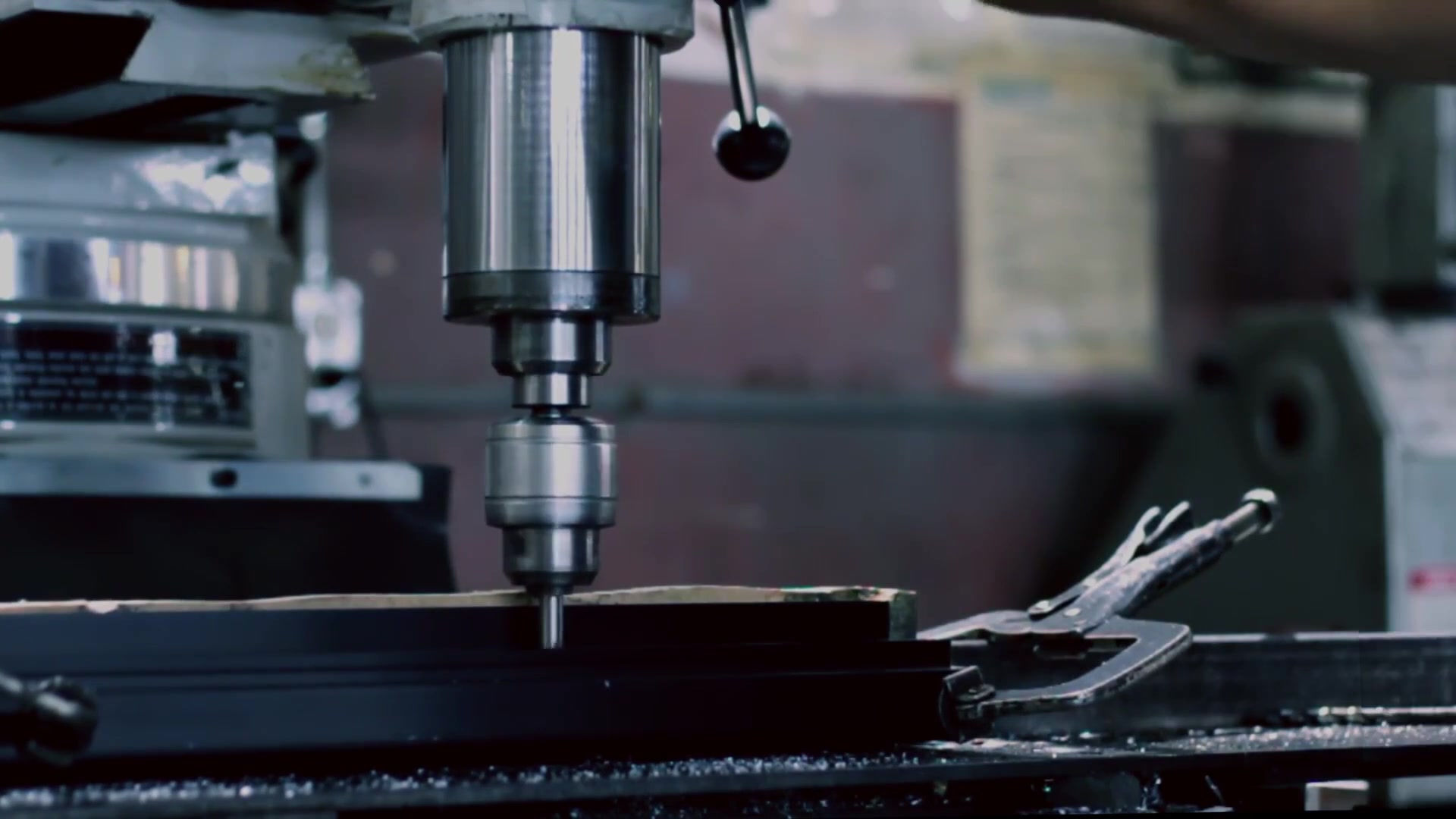
- Electric Discharge Machining, EDM, Spark Machining, Die Sinking
Electric Discharge Machining - EDM - Spark Machining - Die Sinking - Wire Erosion - Custom Manufacturing - AGS-TECH Inc. EDM Machining, Elektrîk-Daxistina Elektrîkê û Çêkirin ELECTRICAL DISCHARGE MACHINING (EDM), also referred to as SPARK-EROSION or ELECTRODISCHARGE MACHINING, SPARK ERODING, DIE SINKING or WIRE EROSION, is a NON-CONVENTIONAL MANUFACTURING process where erosion of metals takes place and desired shape is obtained using electrical discharges in the form of sparks. We also offer some varieties of EDM, namely NO-WEAR EDM, WIRE EDM (WEDM), EDM GRINDING (EDG), DIE-SINKING EDM, ELECTRICAL-DISCHARGE MILLING, micro-EDM, m-EDM and ELECTROCHEMICAL-DISCHARGE GRINDING (ECDG). Our EDM systems consist of shaped tools/electrode and the workpiece connected to DC power supplies and inserted in a electrically nonconducting dielectric fluid. After 1940 electrical discharge machining has become one of the most important and popular production technologies in manufacturing industries. When the distance between the two electrodes is reduced, the intensity of the electric field in the volume between the electrodes becomes greater than the strength of the dielectric in some points, which breaks, eventually forming a bridge for current to flow between the two electrodes. An intense electrical arc is generated causing significant heating to melt a portion of the workpiece and some of the tooling material. As a result, material is removed from both the electrodes. At the same time, the dielectric fluid is heated rapidly, resulting in evaporation of the fluid in the arc gap. Once the current flow stops or it is stopped heat is removed from the gas bubble by the surrounding dielectric fluid and the bubble cavitates (collapses). The shock wave created by the bubble’s collapse and the flow of dielectric fluid flush debris from the workpiece surface and entrain any molten workpiece material into the dielectric fluid. The repetition rate for these discharges are between 50 to 500 kHz, voltages between 50 to 380 V and currents between 0.1 and 500 Amperes. New liquid dielectric such as mineral oils, kerosene or distilled & deionized water is usually conveyed into the inter-electrode volume carrying away the solid particles (in the form of debris) and the insulating proprieties of the dielectric is restored. After a current flow, the potential difference between the two electrodes is restored to what it was before the breakdown, so a new liquid dielectric breakdown can occur. Our modern electrical discharge machines (EDM) offer numerically controlled movements and are equipped with pumps and filtering systems for the dielectric fluids. Electrical discharge machining (EDM) is a machining method mainly used for hard metals or those that would be very difficult to machine with conventional techniques. EDM typically works with any materials that are electrical conductors, although methods for machining insulating ceramics with EDM have also been proposed. The melting point and latent heat of melting are properties that determine the volume of metal removed per discharge. The higher these values, the slower the material removal rate. Because the electrical discharge machining process does not involve any mechanical energy, the hardness, strength, and toughness of the workpiece do not affect the removal rate. Discharge frequency or energy per discharge, the voltage and current are varied to control material removal rates. Rate of material removal and surface roughness increase with increasing current density and decreasing spark frequency. We can cut intricate contours or cavities in pre-hardened steel using EDM without the need for heat treatment to soften and re-harden them. We can use this method with any metal or metal alloys like titanium, hastelloy, kovar, and inconel. Applications of the EDM process include shaping of polycrystalline diamond tools. EDM is considered a non-traditional or non-conventional machining method along with processes such as electrochemical machining (ECM), water jet cutting (WJ, AWJ), laser cutting. On the other hand the conventional machining methods include turning, milling, grinding, drilling and other process whose material removal mechanism is essentially based on mechanical forces. Electrodes for electrical-discharge machining (EDM) are made of graphite, brass, copper and copper-tungsten alloy. Electrode diameters down to 0.1mm are possible. Since tool wear is an undesired phenomenon adversely affecting dimensional accuracy in EDM, we take advantage of a process called NO-WEAR EDM, by reversing polarity and using copper tools to minimize tool wear. Ideally speaking, the electrical-discharge machining (EDM) can be considered a series of breakdown and restoration of the dielectric liquid between the electrodes. In reality however, the removal of the debris from the inter-electrode area is almost always partial. This causes the electrical proprieties of the dielectric in the inter-electrodes area to be different from their nominal values and vary with time. The inter-electrode distance, (spark-gap), is adjusted by the control algorithms of the specific machine used. The spark-gap in EDM can unfortunately sometimes be short-circuited by the debris. The control system of the electrode may fail to react quickly enough to prevent the two electrodes (tool and workpiece) from short circuiting. This unwanted short circuit contributes to material removal differently from the ideal case. We pay utmost importance to flushing action in order to restore the insulating properties of the dielectric so that the current always happens in the point of the inter-electrode area, thereby minimizing the possibility of unwanted change of shape (damage) of the tool-electrode and workpiece. To obtain a specific geometry, the EDM tool is guided along the desired path very close to the workpiece without touching it, We pay utmost attention to the performance of motion control in use. This way, a large number of current discharges / sparks take place, and each contributes to the removal of material from both tool and workpiece, where small craters are formed. The size of the craters is a function of the technological parameters set for the specific job at hand and dimensions may range from the nanoscale (such as in the case of micro-EDM operations) to some hundreds of micrometers in roughing conditions. These small craters on the tool cause gradual erosion of the electrode called “tool wear”. To counteract the detrimental effect of the wear on the geometry of the workpiece we continuously replace the tool-electrode during a machining operation. Sometimes we achieve this by using a continuously replaced wire as electrode ( this EDM process is also called WIRE EDM ). Sometimes we use the tool-electrode in such a way that only a small portion of it is actually engaged in the machining process and this portion is changed on a regular basis. This is, for instance, the case when using a rotating disk as a tool-electrode. This process is called EDM GRINDING. Yet another technique we deploy consists of using a set of electrodes with different sizes and shapes during the same EDM operation to compensate for wear. We call this multiple electrode technique, and is most commonly used when the tool electrode replicates in negative the desired shape and is advanced towards the blank along a single direction, usually the vertical direction (i.e. z-axis). This resembles the sink of the tool into the dielectric liquid in which the workpiece is immersed, and therefore it is referred to as DIE-SINKING EDM (sometimes called CONVENTIONAL EDM or RAM EDM). The machines for this operation are called SINKER EDM. The electrodes for this type of EDM have complex forms. If the final geometry is obtained using a usually simple-shaped electrode moved along several directions and is also subject to rotations, we call it EDM MILLING. The amount of wear is strictly dependent on the technological parameters used in the operation ( polarity, maximum current, open circuit voltage). For example, in micro-EDM, also known as m-EDM, these parameters are usually set at values which generates severe wear. Therefore, wear is a major problem in that area which we minimize using our accumulated know-how. For example to minimize wear to graphite electrodes, a digital generator, controllable within milliseconds, reverses polarity as electro-erosion takes place. This results in an effect similar to electroplating that continuously deposits the eroded graphite back on the electrode. In another method, a so-called ''Zero Wear'' circuit we minimize how often the discharge starts and stops, keeping it on for as long a time as possible. The material removal rate in electrical-discharge machining can be estimated from: MRR = 4 x 10 exp(4) x I x Tw exp (-1.23) Here MRR is in mm3/min, I is current in Amperes, Tw is workpiece melting point in K-273.15K. The exp stands for exponent. On the other hand, the wear rate Wt of the electrode can be obtained from: Wt = ( 1.1 x 10exp(11) ) x I x Ttexp(-2.38) Here Wt is in mm3/min and Tt is melting point of the electrode material in K-273.15K Finally, the wear ratio of the workpiece to electrode R can be obtained from: R = 2.25 x Trexp(-2.38) Here Tr is the ratio of melting points of workpiece to electrode. SINKER EDM : Sinker EDM, also referred to as CAVITY TYPE EDM or VOLUME EDM, consists of an electrode and workpiece submerged in an insulating liquid. The electrode and workpiece are connected to a power supply. The power supply generates an electrical potential between the two. As the electrode approaches the workpiece, dielectric breakdown occurs in the fluid, forming a plasma channel, and a small spark jumps. The sparks usually strike one at a time because it is highly unlikely that different locations in the inter-electrode space have identical local electrical characteristics which would enable a spark to occur in all such locations simultaneously. Hundreds of thousands of these sparks happen at random points between the electrode and the workpiece per second. As the base metal erodes, and the spark gap subsequently increases, the electrode is lowered automatically by our CNC machine so that the process can continue uninterrupted. Our equipment has controlling cycles known as ''on time'' and ''off time''. The on time setting determines the length or duration of the spark. A longer on time produces a deeper cavity for that spark and all subsequent sparks for that cycle, creating a rougher finish on the workpiece and vice versa. The off time is the period of time that one spark is replaced by another. A longer off time permits the dielectric fluid to flush through a nozzle to clean out the eroded debris, thereby avoiding a short circuit. These settings are adjusted in micro seconds. WIRE EDM : In WIRE ELECTRICAL DISCHARGE MACHINING (WEDM), also called WIRE-CUT EDM or WIRE CUTTING, we feed a thin single-strand metal wire of brass through the workpiece, which is submerged in a tank of dielectric fluid. Wire EDM is an important variation of EDM. We occasionally use wire-cut EDM to cut plates as thick as 300mm and to make punches, tools, and dies from hard metals that are difficult to machine with other manufacturing methods. In this process which resembles to contour cutting with a band saw, the wire, which is constantly fed from a spool, is held between upper and lower diamond guides. The CNC-controlled guides move in the x–y plane and the upper guide can also move independently in the z–u–v axis, giving rise to the ability to cut tapered and transitioning shapes (such as circle on the bottom and square at the top). The upper guide can control axis movements in x–y–u–v–i–j–k–l–. This allows the WEDM to cut very intricate and delicate shapes. The average cutting kerf of our equipment that achieves the best economic cost and machining time is 0.335 mm using Ø 0.25 brass, copper or tungsten wire. However the upper and lower diamond guides of our CNC equipment are accurate to about 0.004 mm, and can have a cutting path or kerf as small as 0.021 mm using Ø 0.02 mm wire. So really narrow cuts are possible. The cutting width is greater than the width of the wire because sparking occurs from the sides of the wire to the workpiece, causing erosion. This ''overcut'' is necessary, for many applications it is predictable and therefore can be compensated for ( in micro-EDM this is not often the case). The wire spools are long—an 8 kg spool of 0.25 mm wire is just over 19 kilometers in length. Wire diameter can be as small as 20 micrometres and the geometry precision is in the neighborhood of +/- 1 micrometer. We generally use the wire only once and recycle it because it is relatively inexpensive. It travels at a constant velocity of 0.15 to 9m/min and a constant kerf (slot) is maintained during a cut. In the wire-cut EDM process we use water as the dielectric fluid, controlling its resistivity and other electrical properties with filters and de-ionizer units. The water flushes the cut debris away from the cutting zone. Flushing is an important factor in determining the maximum feed rate for a given material thickness and therefore we keep it consistent. Cutting speed in wire EDM is stated in terms of the cross-sectional area cut per unit time, such as 18,000 mm2/hr for 50mm thick D2 tool steel. The linear cutting speed for this case would be 18,000/50 = 360mm/hr The material removal rate in wire EDM is: MRR = Vf x h x b Here MRR is in mm3/min, Vf is the feed rate of the wire into workpiece in mm/min, h is thickness or height in mm, and b is the kerf, which is: b = dw + 2s Here dw is wire diameter and s is gap between wire and workpiece in mm. Along with tighter tolerances, our modern multi axis EDM wire-cutting machining centers have added features such as multi heads for cutting two parts at the same time, controls for preventing wire breakage, automatic self-threading features in case of wire breakage, and programmed machining strategies to optimize the operation, straight and angular cutting capabilities. Wire-EDM offers us low residual stresses, because it does not require high cutting forces for removal of material. When the energy/power per pulse is relatively low (as in finishing operations), little change in the mechanical properties of a material is expected due to low residual stresses. ELECTRICAL-DISCHARGE GRINDING (EDG) : The grinding wheels do not contain abrasives, they are made of graphite or brass. Repetitive sparks between the rotating wheel and workpiece remove material from workpiece surfaces. The material removal rate is: MRR = K x I Here MRR is in mm3/min, I is current in Amperes, and K is workpiece material factor in mm3/A-min. We frequently use electrical-discharge grinding to saw narrow slits on components. We sometimes combine EDG (Electrical-Discharge Grinding) process with ECG (Electrochemical Grinding) process where material is removed by chemical action, the electrical discharges from the graphite wheel breaking up the oxide film and washed away by the electrolyte. The process is called ELECTROCHEMICAL-DISCHARGE GRINDING (ECDG). Even though the ECDG process consumes relatively more power, it is a faster process than the EDG. We mostly grind carbide tools using this technique. Applications of Electrical Discharge Machining: Prototype production: We use the EDM process in mold-making, tool and die manufacturing, as well as for making prototype and production parts, especially for the aerospace, automobile and electronics industries in which production quantities are relatively low. In Sinker EDM, a graphite, copper tungsten or pure copper electrode is machined into the desired (negative) shape and fed into the workpiece on the end of a vertical ram. Coinage die making: For the creation of dies for producing jewelry and badges by the coinage (stamping) process, the positive master may be made from sterling silver, since (with appropriate machine settings) the master is significantly eroded and is used only once. The resultant negative die is then hardened and used in a drop hammer to produce stamped flats from cutout sheet blanks of bronze, silver, or low proof gold alloy. For badges these flats may be further shaped to a curved surface by another die. This type of EDM is usually performed submerged in an oil-based dielectric. The finished object may be further refined by hard (glass) or soft (paint) enameling and/or electroplated with pure gold or nickel. Softer materials such as silver may be hand engraved as a refinement. Drilling of Small Holes: On our wire-cut EDM machines, we use small hole drilling EDM to make a through hole in a workpiece through which to thread the wire for the wire-cut EDM operation. Separate EDM heads specifically for small hole drilling are mounted on our wire-cut machines which allow large hardened plates to have finished parts eroded from them as needed and without pre-drilling. We also use small hole EDM to drill rows of holes into the edges of turbine blades used in jet engines. Gas flow through these small holes allows the engines to use higher temperatures than otherwise possible. The high-temperature, very hard, single crystal alloys these blades are made of makes conventional machining of these holes with high aspect ratio extremely difficult and even impossible. Other application areas for small hole EDM is to create microscopic orifices for fuel system components. Besides the integrated EDM heads, we deploy stand-alone small hole drilling EDM machines with x–y axes to machine blind or through holes. EDM drills bore holes with a long brass or copper tube electrode that rotates in a chuck with a constant flow of distilled or deionized water flowing through the electrode as a flushing agent and dielectric. Some small-hole drilling EDMs are able to drill through 100 mm of soft or even hardened steel in less than 10 seconds. Holes between 0.3 mm and 6.1 mm can be achieved in this drilling operation. Metal disintegration machining: We also have special EDM machines for the specific purpose of removing broken tools (drill bits or taps) from work pieces. This process is called ''metal disintegration machining''. Advantages and Disadvantages Electrical-Discharge Machining: Advantages of EDM include machining of: - Complex shapes that would otherwise be difficult to produce with conventional cutting tools - Extremely hard material to very close tolerances - Very small work pieces where conventional cutting tools may damage the part from excess cutting tool pressure. - There is no direct contact between tool and work piece. Therefore delicate sections and weak materials can be machined without any distortion. - A good surface finish can be obtained. - Very fine holes can be easily drilled. Disadvantages of EDM include: - The slow rate of material removal. - The additional time and cost used for creating electrodes for ram/sinker EDM. - Reproducing sharp corners on the workpiece is difficult due to electrode wear. - Power consumption is high. - ''Overcut'' is formed. - Excessive tool wear occurs during machining. - Electrically non-conductive materials can be machined only with specific set-up of the process. CLICK Product Finder-Locator Service RÛPERA BERÊ
- Micro-Optics - Micro-Optical - Microoptical - Wafer Level Optics
Micro-Optics, Micro-Optical, Microoptical, Wafer Level Optics, Gratings, Fresnel Lenses, Lens Array, Micromirrors, Micro Reflectors, Collimators, Aspheres, LED Micro-Optics Manufacturing One of the fields in microfabrication we are involved in is MICRO-OPTICS MANUFACTURING. Micro-optics allows the manipulation of light and the management of photons with micron and sub-micron scale structures and components. Some applications of MICRO-OPTICAL COMPONENTS and SUBSYSTEMS are: Information technology: In micro-displays, micro-projectors, optical data storage, micro-cameras, scanners, printers, copiers…etc. Biomedicine: Minimally-invasive/point of care diagnostics, treatment monitoring, micro-imaging sensors, retinal implants, micro-endoscopes. Lighting: Systems based on LEDs and other efficient light sources Safety and Security Systems: Infrared night vision systems for automotive applications, optical fingerprint sensors, retinal scanners. Optical Communication & Telecommunication: In photonic switches, passive fiber optic components, optical amplifiers, mainframe and personal computer interconnect systems Smart structures: In optical fiber-based sensing systems and much more The types of micro-optical components and subsystems we manufacture and supply are: - Wafer Level Optics - Refractive Optics - Diffractive Optics - Filters - Gratings - Computer Generated Holograms - Hybrid Microoptical Components - Infrared Micro-Optics - Polymer Micro-Optics - Optical MEMS - Monolithically and Discretely Integrated Micro-Optic Systems Some of our most widely used micro-optical products are: - Bi-convex and plano-convex lenses - Achromat lenses - Ball lenses - Vortex Lenses - Fresnel Lenses - Multifocal Lens - Cylindrical Lenses - Graded Index (GRIN) Lenses - Micro-Optical Prisms - Aspheres - Arrays of Aspheres - Collimators - Micro-Lens Arrays - Diffraction Gratings - Wire-Grid Polarizers - Micro-Optic Digital Filters - Pulse Compression Gratings - LED Modules - Beam Shapers - Beam Sampler - Ring Generator - Micro-Optical Homogenizers / Diffusers - Multispot Beam Splitters - Dual Wavelength Beam Combiners - Micro-Optical Interconnects - Intelligent Micro-Optics Systems - Imaging Microlenses - Micromirrors - Micro Reflectors - Micro-Optical Windows - Dielectric Mask - Iris Diaphragms Let us provide you some basic information about these micro-optical products and their applications: BALL LENSES: Ball lenses are completely spherical micro-optic lenses most commonly used to couple light in and out of fibers. We supply a range of micro-optic stock ball lenses and can manufacture also to your own specifications. Our stock ball lenses from quartz have excellent UV and IR transmission between 185nm to >2000nm, and our sapphire lenses have a higher refractive index, allowing a very short focal length for excellent fiber coupling. Micro-optical ball lenses from other materials and diameters are available. Besides fiber coupling applications, micro-optical ball lenses are used as objective lenses in endoscopy, laser measurement systems and bar-code scanning. On the other hand, micro-optic half ball lenses offer uniform dispersion of light and are widely used in LED displays and traffic lights. MICRO-OPTICAL ASPHERES and ARRAYS: Aspheric surfaces have a non-spherical profile. Use of aspheres can reduce the number of optics required to reach a desired optical performance. Popular applications for micro-optical lens arrays with spherical or aspherical curvature are imaging and illumination and the effective collimation of laser light. Substitution of a single aspheric microlens array for a complex multilens system results not only in smaller size, lighter weight, compact geometry, and lower cost of an optical system, but also in significant improvement of its optical performance such as better imaging quality. However, the fabrication of aspheric microlenses and microlens arrays is challenging, because conventional technologies used for macro-sized aspheres like single-point diamond milling and thermal reflow are not capable of defining a complicated micro-optic lens profile in an area as small as several to tens of micrometers. We possess the know-how of producing such micro-optical structures using advanced techniques such as femtosecond lasers. MICRO-OPTICAL ACHROMAT LENSES: These lenses are ideal for applications requiring color correction, while aspheric lenses are designed to correct spherical aberration. An achromatic lens or achromat is a lens that is designed to limit the effects of chromatic and spherical aberration. Micro-optical achromatic lenses make corrections to bring two wavelengths (such as red and blue colors) into focus on the same plane. CYLINDRICAL LENSES: These lenses focus light into a line instead of a point, as a spherical lens would. The curved face or faces of a cylindrical lens are sections of a cylinder, and focus the image passing through it into a line parallel to the intersection of the surface of the lens and a plane tangent to it. The cylindrical lens compresses the image in the direction perpendicular to this line, and leaves it unaltered in the direction parallel to it (in the tangent plane). Tiny micro-optical versions are available which are suitable for use in micro optical environments, requiring compact-size fiber optical components, laser systems, and micro-optical devices. MICRO-OPTICAL WINDOWS and FLATS: Milimetric micro-optical windows meeting tight tolerance requirements are available. We can custom manufacture them to your specifications from any of the optical grade glasses. We offer a variety of micro-optical windows made of different materials such as fused silica, BK7, sapphire, zinc sulphide….etc. with transmission from UV to middle IR range. IMAGING MICROLENSES: Microlenses are small lenses, generally with a diameter less than a millimetre (mm) and as small as 10 micrometres. Imaging Lenses are used to view objects in imaging systems. Imaging Lenses are used in imaging systems to focus an image of an examined object onto a camera sensor. Depending on the lens, imaging lenses can be used to remove parallax or perspective error. They can also offer adjustable magnifications, field of views, and focal lengths. These lenses allow an object to be viewed in several ways to illustrate certain features or characteristics that may be desirable in certain applications. MICROMIRRORS: Micromirror devices are based on microscopically small mirrors. The mirrors are Microelectromechanical systems (MEMS). The states of these micro-optical devices are controlled by applying a voltage between the two electrodes around the mirror arrays. Digital micromirror devices are used in video projectors and optics and micromirror devices are used for light deflection and control. MICRO-OPTIC COLLIMATORS & COLLIMATOR ARRAYS: A variety of micro-optical collimators are available off-the-shelf. Micro-optical small beam collimators for demanding applications are produced using laser fusion technology. The fiber end is directly fused to the optical center of the lens, thereby eliminated epoxy within the optical path. The micro-optic collimator lens surface is then laser polished to within a millionth of an inch of the ideal shape. Small Beam collimators produce collimated beams with beam waists under a millimeter. Micro-optical small beam collimators are typically used at 1064, 1310 or 1550 nm wavelengths. GRIN lens based micro-optic collimators are also available as well as collimator array and collimator fiber array assemblies. MICRO-OPTICAL FRESNEL LENSES: A Fresnel lens is a type of compact lens designed to allow the construction of lenses of large aperture and short focal length without the mass and volume of material that would be required by a lens of conventional design. A Fresnel lens can be made much thinner than a comparable conventional lens, sometimes taking the form of a flat sheet. A Fresnel lens can capture more oblique light from a light source, thus allowing the light to be visible over greater distances. The Fresnel lens reduces the amount of material required compared to a conventional lens by dividing the lens into a set of concentric annular sections. In each section, the overall thickness is decreased compared to an equivalent simple lens. This can be viewed as dividing the continuous surface of a standard lens into a set of surfaces of the same curvature, with stepwise discontinuities between them. Micro-optic Fresnel lenses focus light by refraction in a set of concentric curved surfaces. These lenses can be made very thin and lightweight. Micro-optical Fresnel lenses offer opportunities in optics for highresolution Xray applications, throughwafer optical interconnection capabilities. We have a number of fabrication methods including micromolding and micromachining to manufacture micro-optical Fresnel lenses and arrays specifically for your applications. We can design a positive Fresnel lens as a collimator, collector or with two finite conjugates. Micro-Optical Fresnel lenses are usually corrected for spherical aberrations. Micro-optic positive lenses can be metalized for use as a second surface reflector and negative lenses can be metalized for use as a first surface reflector. MICRO-OPTICAL PRISMS: Our line of precision micro-optics includes standard coated and uncoated micro prisms. They are suitable for use with laser sources and imaging applications. Our micro-optical prisms have submilimeter dimensions. Our coated micro-optical prisms can also be used as mirror reflectors with respect to incoming light. Uncoated prisms act as mirrors for light incident on one of the short sides since incident light is totally internally reflected at the hypotenuse. Examples of our micro-optical prism capabilities include right angle prisms, beamsplitter cube assemblies, Amici prisms, K-prisms, Dove prisms, Roof prisms, Cornercubes, Pentaprisms, Rhomboid prisms, Bauernfeind prisms, Dispersing prisms, Reflecting prisms. We also offer light guiding and de-glaring optical micro-prisms made from acrylic, polycarbonate and other plastic materials by hot embossing manufacturing process for applications in lamps and luminaries, LEDs. They are highly efficient, strong light guiding precise prism surfaces, support luminaries to fulfill office regulations for de-glaring. Additional customized prism structures are possible. Microprisms and microprism arrays on wafer level are also possible using microfabrication techniques. DIFFRACTION GRATINGS: We offer design and manufacture of diffractive micro-optical elements (DOEs). A diffraction grating is an optical component with a periodic structure, which splits and diffracts light into several beams travelling in different directions. The directions of these beams depend on the spacing of the grating and the wavelength of the light so that the grating acts as the dispersive element. This makes grating a suitable element to be used in monochromators and spectrometers. Using wafer-based lithography, we produce diffractive micro-optical elements with exceptional thermal, mechanical and optical performance characteristics. Wafer-level processing of micro-optics provides excellent manufacturing repeatability and economic output. Some of the available materials for diffractive micro-optical elements are crystal-quartz, fused-silica, glass, silicon and synthetic substrates. Diffraction gratings are useful in applications such as spectral analysis / spectroscopy, MUX/DEMUX/DWDM, precision motion control such as in optical encoders. Lithography techniques make the fabrication of precision micro-optical gratings with tightly-controlled groove spacings possible. AGS-TECH offers both custom and stock designs. VORTEX LENSES: In laser applications there is a need to convert a Gaussian beam to a donut-shaped energy ring. This is achieved using Vortex lenses. Some applications are in lithography and high-resolution microscopy. Polymer on glass Vortex phase plates are also available. MICRO-OPTICAL HOMOGENIZERS / DIFFUSERS: A variety of technologies are used to fabricate our micro-optical homogenizers and diffusers, including embossing, engineered diffuser films, etched diffusers, HiLAM diffusers. Laser Speckle is the optical phenomena resulting from the random interference of coherent light. This phenomenon is utilized to measure the Modulation Transfer Function (MTF) of detector arrays. Microlens diffusers are shown to be efficient micro-optic devices for speckle generation. BEAM SHAPERS: A micro-optic beam shaper is an optic or a set of optics that transforms both the intensity distribution and the spatial shape of a laser beam to something more desirable for a given application. Frequently, a Gaussian-like or non-uniform laser beam is transformed to a flat top beam. Beam shaper micro-optics are used to shape and manipulate single mode and multi-mode laser beams. Our beam shaper micro-optics provide circular, square, rectilinear, hexagonal or line shapes, and homogenize the beam (flat top) or provide a custom intensity pattern according to the requirements of the application. Refractive, diffractive and reflective micro-optical elements for laser beam shaping and homogenizing have been manufactured. Multifunctional micro-optical elements are used for shaping arbitrary laser beam profiles into a variety of geometries like, a homogeneous spot array or line pattern, a laser light sheet or flat-top intensity profiles. Fine beam application examples are cutting and keyhole welding. Broad beam application examples are conduction welding, brazing, soldering, heat treatment, thin film ablation, laser peening. PULSE COMPRESSION GRATINGS: Pulse compression is a useful technique that takes advantage of the relationship between pulse duration and spectral width of a pulse. This enables the amplification of laser pulses above the normal damage threshold limits imposed by the optical components in the laser system. There are linear and nonlinear techniques for reducing the durations of optical pulses. There is variety of methods for temporally compressing / shortening optical pulses, i.e., reducing the pulse duration. These methods generally start in the picosecond or femtosecond region, i.e. already in the regime of ultrashort pulses. MULTISPOT BEAM SPLITTERS: Beam splitting by means of diffractive elements is desirable when one element is required to produce several beams or when very exact optical power separation is required. Precise positioning can also be achieved, for example, to create holes at clearly defined and accurate distances. We have Multi-Spot Elements, Beam Sampler Elements, Multi-Focus Element. Using a diffractive element, collimated incident beams are split into several beams. These optical beams have equal intensity and equal angle to one another. We have both one-dimensional and two-dimensional elements. 1D elements split beams along a straight line whereas 2D elements produce beams arranged in a matrix of, for example, 2 x 2 or 3 x 3 spots and elements with spots that are arranged hexagonally. Micro-optical versions are available. BEAM SAMPLER ELEMENTS: These elements are gratings that are used for inline monitoring of high power lasers. The ± first diffraction order can be used for beam measurements. Their intensity is significantly lower than that of the main beam and can be custom designed. Higher diffraction orders can also be used for measurement with even lower intensity. Variations in intensity and changes in the beam profile of high power lasers can be reliably monitored inline using this method. MULTI-FOCUS ELEMENTS: With this diffractive element several focal points can be created along the optical axis. These optical elements are used in sensors, ophthalmology, material processing. Micro-optical versions are available. MICRO-OPTICAL INTERCONNECTS: Optical interconnects have been replacing electrical copper wires at the different levels in the interconnect hierarchy. One of the possibilities to bring the advantages of micro-optics telecommunications to the computer backplane, the printed circuit board, the inter-chip and on-chip interconnect level, is to use free-space micro-optical interconnect modules made of plastic. These modules are capable of carrying high aggregate communication bandwidth through thousands of point-to-point optical links on a footprint of a square centimeter. Contact us for off-shelf as well as custom tailored micro-optical interconnects for computer backplane, the printed circuit board, the inter-chip and on-chip interconnect levels. INTELLIGENT MICRO-OPTICS SYSTEMS: Intelligent micro-optic light modules are used in smart phones and smart devices for LED flash applications, in optical interconnects for transporting data in supercomputers and telecommunications equipment, as miniaturized solutions for near-infrared beam shaping, detection in gaming applications and for supporting gesture control in natural user interfaces. Sensing opto-electronic modules are used for a number of product applications such as ambient light and proximity sensors in smart phones. Intelligent imaging micro-optic systems are used for primary and front-facing cameras. We offer also customized intelligent micro-optical systems with high performance and manufacturability. LED MODULES: You can find our LED chips, dies and modules on our page Lighting & Illumination Components Manufacturing by clicking here. WIRE-GRID POLARIZERS: These consist of a regular array of fine parallel metallic wires, placed in a plane perpendicular to the incident beam. The polarization direction is perpendicular to the wires. Patterned polarizers have applications in polarimetry, interferometry, 3D displays, and optical data storage. Wire-grid polarizers are extensively used in infrared applications. On the other hand micropatterned wire-grid polarizers have limited spatial resolution and poor performance at visible wavelengths, are susceptible to defects and cannot be easily extended to non-linear polarizations. Pixelated polarizers use an array of micro-patterned nanowire grids. The pixelated micro-optical polarizers can be aligned with cameras, plane arrays, interferometers, and microbolometers without the need for mechanical polarizer switches. Vibrant images distinguishing between multiple polarizations across the visible and IR wavelengths can be captured simultaneously in real-time enabling fast, high resolution images. Pixelated micro-optical polarizers also enable clear 2D and 3D images even in low-light conditions. We offer patterned polarizers for two, three and four-state imaging devices. Micro-optical versions are available. GRADED INDEX (GRIN) LENSES: Gradual variation of the refractive index (n) of a material can be used to produce lenses with flat surfaces, or lenses that do not have the aberrations typically observed with traditional spherical lenses. Gradient-index (GRIN) lenses may have a refraction gradient that is spherical, axial, or radial. Very small micro-optical versions are available. MICRO-OPTIC DIGITAL FILTERS: Digital neutral density filters are used to control the intensity profiles of illumination and projection systems. These micro-optic filters contain well-defined metal absorber micro-structures that are randomly distributed on a fused silica substrate. Properties of these micro-optical components are high accuracy, large clear aperture, high damage threshold, broadband attenuation for DUV to IR wavelengths, well defined one or two dimensional transmission profiles. Some applications are soft edge apertures, precise correction of intensity profiles in illumination or projection systems, variable attenuation filters for high-power lamps and expanded laser beams. We can customize the density and size of the structures to meet precisely the transmission profiles required by the application. MULTI-WAVELENGTH BEAM COMBINERS: Multi-Wavelength beam combiners combine two LED collimators of different wavelengths into a single collimated beam. Multiple combiners can be cascaded to combine more than two LED collimator sources. Beam combiners are made of high-performance dichroic beam splitters that combine two wavelengths with >95% efficiency. Very small micro-optic versions are available. CLICK Product Finder-Locator Service RÛPERA BERÊ
- Active Optical Components, Lasers, Photodetectors, LED Dies, Laser
Active Optical Components - Lasers - Photodetectors - LED Dies - Photomicrosensor - Fiber Optic - AGS-TECH Inc. - USA Hilberîn & Civîna Pêkhateyên Optîk ên Çalak The ACTIVE OPTICAL COMPONENTS we manufacture and supply are: • Lasers and photodetectors, PSD (Position Sensitive Detectors), quadcells and other optical sensors and sensor systems with electrical connections. Our active optical components span a large spectrum of wavelength regions. Whether your application is high power lasers for industrial cutting, drilling, welding...etc, or medical lasers for surgery or diagnostics, or telecommunication lasers or detectors suitable for the ITU grid, we are your one-stop source. Below are downloadable brochures for some of our off-the-shelf active optical components and devices. If you cannot find what you are searching for, please contact us and we will have something to offer you. We do also custom manufacture active optical components and assemblies according to your application and requirements. • Among the many achievements of our optical engineers is the concept design, optical and opto-mechanical design of optical scan head for GS 600 LASER DRILLING SYSTEM with dual galvo scanners and self compensating alignment. Since its introduction, the GS600 family has become the system of choice for many leading high volume manufacturers around the World. Using optical design tools such as ZEMAX and CodeV, our optical engineers are ready to design your custom systems. If you only have SOLIDWORKS files for your design, don't worry, send them and we will work out and create the optical design files, optimize & simulate and have you approve the final design. Even a hand sketch, a mockup, a prototype or sample is sufficient in most cases for us to take care of your product development needs. Click on blue highlighted text to download brochures and catalogs of some off-the-shelf-ready active optical products: Active fiber optic products Comprehensive electric & electronic components catalog for off-shelf products Hikrobot Machine Vision Products Hikrobot Smart Machine Vision Products Hikrobot Machine Vision Standard Products Hikvision Logistic Vision Solutions LED dies and chips Photomicrosensors Photosensors Photosensors and Photomicrosensors Sockets and Accessories Private Label Medical Endoscopes and Visualization Systems (We can put your company name and logo on these) Sensors & Analytical Measurement Systems for Optical OEM Applications in Liquid Analysis (We private label these with your brand name and logo if you wish. We can customize sensors to your needs and applications, OEM option available) Dowload brochure for our DESIGN PARTNERSHIP PROGRAM R e ference Code: OICASANLY CLICK Product Finder-Locator Service RÛPERA BERÊ
- Industrial Servers, Database Server, File Server, Mail Server, Print
Industrial Servers - Database Server - File Server - Mail Server - Print Server - Web Server - AGS-TECH Inc. - NM - USA Pêşkêşkerên Pîşesazî When referring to client-server architecture, a SERVER is a computer program that runs to serve the requests of other programs, also considered as the ''clients''. In other words the ''server'' performs computational tasks on behalf of its ''clients''. The clients may either run on the same computer or be connected through the network. In popular use however, a server is a physical computer dedicated to running as a host one or more of these services and to serve the needs of users of the other computers on the network. A server could be a DATABASE SERVER, FILE SERVER, MAIL SERVER, PRINT SERVER, WEB SERVER, or else depending on the computing service it offers. We offer the best quality industrial server brands available such as ATOP TECHNOLOGIES, KORENIX and JANZ TEC . Click on blue highlighted text below to download respective catalogs and brochures: - ATOP TECHNOLOGIES compact product brochure - ATOP Technologies Product List 2021) - ICP DAS brand industrial communication and networking products brochure - ICP DAS brand Tiny Device Server and Modbus Gateway brochure - JANZ TEC brand compact product brochure - KORENIX brand compact product brochure To choose a suitable Industrial Grade Server, please go to our industrial computer store by CLICKING HERE. Dowload brochure for our DESIGN PARTNERSHIP PROGRAM DATABASE SERVER : This term is used to refer to the back-end system of a database application using client/server architecture. The back-end database server performs tasks such as data analysis, data storage, data manipulation, data archiving, and other non-user specific tasks. FILE SERVER : In the client/server model, this is a computer responsible for the central storage and management of data files so that other computers on the same network can access them. File servers allow users to share information over a network without physically transferring files by floppy disk or other external storage devices. In sophisticated and professional networks, a file server might be a dedicated network-attached storage (NAS) device that also serves as a remote hard disk drive for other computers. Thus anyone on the network can store files on it like to their own hard drive. MAIL SERVER : A mail server, also called an e-mail server is a computer within your network that works as your virtual post office. It consists of a storage area where e-mail is stored for local users, a set of user defined rules determining how the mail server should react to the destination of a specific message, a database of user accounts that the mail server will recognize and deal with locally, and communications modules which handle the transfer of messages to and from other email servers and clients. Mail servers are generally designed to operate with no manual intervention during normal operation. PRINT SERVER : Sometimes called a printer server, this is a device that connects printers to client computers over a network. Print servers accept print jobs from the computers and send the jobs to the appropriate printers. Print server queues jobs locally because work may arrive more quickly than the printer can actually handle it. WEB SERVER : These are computers that deliver and serve Web pages. All Web servers have IP addresses and generally domain names. When we enter the URL of a website in our browser, this sends a request to the Web server whose domain name is the website entered. The server then fetches the page named index.html and sends it to our browser. Any computer can be turned into a Web server by installing server software and connecting the machine to the Internet. There are many Web server software applications such as packages from Microsoft and Netscape. CLICK Product Finder-Locator Service RÛPERA BERÊ
- Test Equipment for Testing Paper & Packaging Products
Test Equipment for Testing Paper & Packaging Products, Adhesive Tape Peel Test Machine, Carton Compressive Tester, Foam Compression Hardness Tester, Zero Drop Test Machine, Package Incline Impact Tester Amûrên ceribandinê ji bo ceribandina kaxez û hilberên pakkirinê Specialized Test Equipment for Testing of Paper & Packaging Products are used for testing paper & packaging products such as cardboard boxes, carton materials, foam and cushioning materials and other types of packages....etc., for checking their quality, endurance, functionality, reliability, safety, compliance to domestic and international standards....etc. Our specialized test equipment can be either: - CUSTOM DESIGNED and MANUFACTURED SPECIALIZED TEST EQUIPMENT for PAPER & PACKAGING TESTING or - OFF-SHELF SPECIALIZED TEST EQUIPMENT for PAPER & PACKAGING TESTING Custom designed specialized testing equipment is designed and developed by us for our customers specific needs, taking into consideration our customers specific requirements, their markets, their legal responsibilities...etc. We work with you hand in hand to accomplish what you need and want. Our engineers design, prototype and get your approval prior to manufacturing your test machines. On the other hand, our off-shelf specialized test equipment for testing of Paper & Packaging Products are already designed and manufactured systems that can be purchased quickly from us and used. If you let us know what you need, we will be happy to guide you and propose you ready systems that can help achieve your goals. Our off-shelf specialized test equipment for testing of Paper & Packaging Products can be downloaded from the colored links below: HAIDA Adhesive Tape Peel Test Machine HAIDA Automatic Bursting Strength Test Machine HAIDA Bursting Strength Tester Series HAIDA Clamping Force Testing Machine HAIDA Computer Servo Carton Compressive Tester Series HAIDA Double-Column Drop Test Machine HAIDA Foam Compression Hardness Tester HAIDA Foam Pounding Fatigue Tester HAIDA Foam Rebound Test Machine HAIDA Foam Tear Resistance Tester HAIDA Four Point Bending Stiffness Tester HAIDA Microcomputer Carton Compressive Tester Series HAIDA Microcomputer Ring Crush & Edge HAIDA Package Incline Impact Tester HAIDA Paper Four Point Bending Resistance Tester HAIDA Ring Crush & Edge Crush Tester Series HAIDA Single Drop Test Machine HAIDA Universal Packaging Material Testing Machine HAIDA Zero Drop Test Machine Ji bo alavên din ên bi vî rengî, ji kerema xwe biçin malpera alavên me: http://www.sourceindustrialsupply.com CLICK Product Finder-Locator Service RÛPERA BERÊ
- Coating Thickness Gauge, Surface Roughness Tester, Nondestructive Test
Coating Thickness Gauge - Surface Roughness Tester - Nondestructive Testing - SADT - Mitech - AGS-TECH Inc. - NM - USA Amûrên Testê yên Rakirina Rûyê Among our test instruments for coating and surface evaluation are COATING THICKNESS METERS, SURFACE ROUGHNESS TESTERS, GLOSS METERS, COLOR READERS, COLOR DIFFERENCE METER, METALLURGICAL MICROSCOPES, INVERTED METALLOGRAPHIC MICROSCOPE. Our main focus is on NON-DESTRUCTIVE TEST METHODS. We carry high quality brands such as ELCOMETER, SADT-SINOAGE and MITECH. A large percentage of all surfaces around us are coated. Coatings serve many purposes including good appearance, protection and giving products certain desired functionality such as water repelling, enhanced friction, wear and abrasion resistance….etc. Therefore it is of vital importance to be capable to measure, test and evaluate the properties and quality of coatings and surfaces of products. Coatings can be broadly categorized into two main groups if thicknesses are taken into consideration: THICK FILM and THIN FILM COATINGS. Please click on highlighted text below to download respective catalogs. You can procure brand new, or refurbished and used surface coating test instruments from us. Simply indicate the brand name, model number and we will provide you the most competitive quote. AMETEK-LLOYD Instruments Materials Testing (does include also Peeling, Adhesion Test Instruments...etc.) ELCOMETER Inspection Equipment (many coating inspection instruments available) HAIDA Color Assessment Cabinet MI TECH Coating Thickness Gauge Model MCT200 catalog. SADT-SINOAGE Brand Metrology and Test Equipment catalog download. In this catalog you will find some of these instruments for the evaluation of surfaces and coatings. Some of the instruments and techniques used for such purposes are: COATING THICKNESS METER : Different types of coatings require different types of coating testers. A basic understanding of the various techniques is thus essential for the user to choose the right equipment. In the Magnetic Induction Method of coating thickness measurement we measure nonmagnetic coatings over ferrous substrates and magnetic coatings over nonmagnetic substrates. The probe is positioned on the sample and the linear distance between the probe tip that contacts the surface and the base substrate is measured. Inside the measurement probe is a coil that generates a changing magnetic field. When the probe is placed on the sample, the magnetic flux density of this field is altered by the thickness of a magnetic coating or the presence of a magnetic substrate. The change in magnetic inductance is measured by a secondary coil on the probe. The output of the secondary coil is transferred to a microprocessor, where it’s shown as a coating thickness measurement on the digital display. This quick test is suitable for liquid or powder coatings, platings such as chrome, zinc, cadmium or phosphate over steel or iron substrates. Coatings such as paint or powder thicker than 0.1 mm are suitable for this method. The magnetic induction method is not well suited for nickel over steel coatings because of nickel’s partial magnetic property. Phase-sensitive Eddy current method is more suitable for these coatings. Another type of coating where the magnetic induction method is prone to failure is zinc galvanized steel. The probe will read a thickness equal to the total thickness. Newer model instruments are capable of self-calibration by detecting the substrate material through the coating. This is of course very helpful when a bare substrate is not available or when the substrate material is unknown. Cheaper equipment versions require however calibration of the instrument on a bare and uncoated substrate. The Eddy Current Method of coating thickness measurement measures nonconductive coatings on nonferrous conductive substrates, nonferrous conductive coatings on nonconductive substrates and some nonferrous metal coatings on nonferrous metals. It is similar to the magnetic inductive method previously mentioned containing a coil and similar probes. The coil in the Eddy current method has the dual function of excitation and measurement. This probe coil is driven by a high-frequency oscillator to generate an alternating high-frequency field. When placed near a metallic conductor, eddy currents are generated in the conductor. Impedance change takes place in the probe coil. The distance between the probe coil and the conductive substrate material determines the amount of impedance change, which can be measured, correlated to a coating thickness and displayed in the form of a digital reading. Applications include liquid or powder coating on aluminum and nonmagnetic stainless steel, and anodize over aluminum. This method’s reliability depends on the part’s geometry and the coating’s thickness. The substrate needs to be known prior to taking readings. Eddy current probes shouldn’t be used for measuring nonmagnetic coatings over magnetic substrates such as steel and nickel over aluminum substrates. If users must measure coatings over magnetic or nonferrous conductive substrates they will be best served with a dual magnetic induction/Eddy current gage that automatically recognizes the substrate. A third method, called the Coulometric method of coating thickness measurement, is a destructive testing method that has many important functions. Measuring the duplex nickel coatings in the automotive industry is one of it major applications. In the coulometric method, the weight of an area of known size on a metallic coating is determined through localized anodic stripping of the coating. The mass-per-unit area of the coating thickness is then calculated. This measurement on the coating is made using an electrolysis cell, which is filled with an electrolyte specifically selected to strip the particular coating. A constant current runs through the test cell, and since the coating material serves as the anode, it gets deplated. The current density and the surface area are constant, and thus the coating thickness is proportional to the time it takes to strip and take off the coating. This method is very useful for measuring electrically conductive coatings on a conductive substrate. The Coulometric method can also be used for determining the coating thickness of multiple layers on a sample. For example, the thickness of nickel and copper can be measured on a part with a top coating of nickel and an intermediate copper coating on a steel substrate. Another example of a multilayer coating is chrome over nickel over copper on top of a plastic substrate. Coulometric test method is popular in electroplating plants with a small number of random samples. Yet a fourth method is the Beta Backscatter Method for measuring coating thicknesses. A beta-emitting isotope irradiates a test sample with beta particles. A beam of beta particles is directed through an aperture onto the coated component, and a proportion of these particles are backscattered as expected from the coating through the aperture to penetrate the thin window of a Geiger Muller tube. The gas in the Geiger Muller tube ionizes, causing a momentary discharge across the tube electrodes. The discharge which is in the form of a pulse is counted and translated to a coating thickness. Materials with high atomic numbers backscatter the beta particles more. For a sample with copper as a substrate and a gold coating of 40 microns thick, the beta particles are scattered by both the substrate and the coating material. If the gold coating thickness increases, the backscatter rate also increases. The change in the rate of particles scattered is therefore a measure of the coating thickness. Applications that are suitable for the beta backscatter method are those where the atomic number of the coating and substrate differ by 20 percent. These include gold, silver or tin on electronic components, coatings on machine tools, decorative platings on plumbing fixtures, vapor-deposited coatings on electronic components, ceramics and glass, organic coatings such as oil or lubricant over metals. The beta backscatter method is useful for thicker coatings and for substrate & coating combinations where magnetic induction or Eddy current methods won’t work. Changes in alloys affect the beta backscatter method, and different isotopes and multiple calibrations might be required to compensate. An example would be tin/lead over copper, or tin over phosphorous/bronze well known in printed circuit boards and contact pins, and in these cases the changes in alloys would be better measured with the more expensive X-ray fluorescence method. The X-ray fluorescence method for measuring coating thickness is a noncontact method that allows the measurement of very thin multilayer alloy coatings on small and complex parts. Parts are exposed to X-radiation. A collimator focuses the X-rays onto an exactly defined area of the test specimen. This X-radiation causes characteristic X-ray emission (i.e., fluorescence) from both the coating and the substrate materials of the test specimen. This characteristic X-ray emission is detected with an energy dispersive detector. Using the appropriate electronics, it’s possible to register only the X-ray emission from the coating material or substrate. It’s also possible to selectively detect a specific coating when intermediate layers are present. This technique is widely used on printed circuit boards, jewelry and optical components. The X-ray fluorescence is not suitable for organic coatings. The measured coating’s thickness should not exceed 0.5-0.8 mils. However, unlike the beta backscatter method, X-ray fluorescence can measure coatings with similar atomic numbers (for example nickel over copper). As previously mentioned, different alloys affect an instrument’s calibration. Analyzing base material and coating’s thickness are critical for ensuring precision readings. Todays systems and software programs reduce the need for multiple calibrations without sacrificing quality. Finally it is worth mentioning that there are gages that can operate in several of the above mentioned modes. Some have detachable probes for flexibility in use. Many of these modern instruments do offer statistical analysis capabilities for process control and minimal calibration requirements even if used on differently shaped surfaces or different materials. SURFACE ROUGHNESS TESTERS : Surface roughness is quantified by the deviations in the direction of the normal vector of a surface from its ideal form. If these deviations are large, the surface is considered rough; if they are small, the surface is considered smooth. Commercially available instruments called SURFACE PROFILOMETERS are used to measure and record surface roughness. One of the commonly used instruments features a diamond stylus traveling along a straight line over the surface. The recording instruments are able to compensate for any surface waviness and indicate only roughness. Surface roughness can be observed through a.) Interferometry and b.) Optical microscopy, scanning-electron microscopy, laser or atomic-force microscopy (AFM). Microscopy techniques are especially useful for imaging very smooth surfaces for which features cannot be captured by less sensitive instruments. Stereoscopic photographs are useful for 3D views of surfaces and can be used to measure surface roughness. 3D surface measurements can be performed by three methods. Light from an optical-interference microscope shines against a reflective surface and records the interference fringes resulting from the incident and reflected waves. Laser profilometers are used to measure surfaces through either interferometric techniques or by moving an objective lens to maintain a constant focal length over a surface. The motion of the lens is then a measure of the surface. Lastly, the third method, namely the atomic-force microscope, is used for measuring extremely smooth surfaces on the atomic scale. In other words with this equipment even atoms on the surface can be distinguished. This sophisticated and relatively expensive equipment scans areas of less than 100 micron square on specimen surfaces. GLOSS METERS, COLOR READERS, COLOR DIFFERENCE METER : A GLOSSMETERmeasures the specular reflection gloss of a surface. A measure of gloss is obtained by projecting a light beam with fixed intensity and angle onto a surface and measuring the reflected amount at an equal but opposite angle. Glossmeters are used on a variety of materials such as paint, ceramics, paper, metal and plastic product surfaces. Measuring gloss can serve companies in assuring quality of their products. Good manufacturing practices require consistency in processes and this includes consistent surface finish and appearance. Gloss measurements are carried out at a number of different geometries. This depends on the surface material. For example metals have high levels of reflection and therefore the angular dependence is less as compared to non-metals such as coatings and plastics where angular dependence is higher due to diffuse scattering and absorption. Illumination source and observation reception angles configuration allows measurement over a small range of the overall reflection angle. The measurement results of a glossmeter are related to the amount of reflected light from a black glass standard with a defined refractive index. The ratio of the reflected light to the incident light for the test specimen, compared to the ratio for the gloss standard, is recorded as gloss units (GU). Measurement angle refers to the angle between the incident and reflected light. Three measurement angles (20°, 60°, and 85°) are used for the majority of industrial coatings. The angle is selected based on the anticipated gloss range and the following actions are taken depending on the measurement: Gloss Range..........60° Value.......Action High Gloss............>70 GU..........If measurement exceeds 70 GU, change test setup to 20° to optimize measurement accuracy. Medium Gloss........10 - 70 GU Low Gloss.............<10 GU..........If measurement is less than 10 GU, change test setup to 85° to optimize measurement accuracy. Three types of instruments are available commercially: 60° single angle instruments, a double-angle type that combines 20° and 60° and a triple-angle type that combines 20°, 60° and 85°. Two additional angles are used for other materials, the angle of 45° is specified for the measurement of ceramics, films, textiles and anodized aluminum, while the measurement angle 75° is specified for paper and printed materials. A COLOR READER or also referred to as COLORIMETER is a device that measures the absorbance of particular wavelengths of light by a specific solution. Colorimeters are most commonly used to determine the concentration of a known solute in a given solution by the application of the Beer-Lambert law, which states that the concentration of a solute is proportional to the absorbance. Our portable color readers can also be used on plastic, painting, platings, textiles, printing, dye making, food such as butter, french fries, coffee, baked products and tomatoes….etc. They can be used by amateurs who don’t have professional knowledge on colors. Since there are many types of color readers, the applications are endless. In quality control they are used mainly to insure samples fall within color tolerances set by the user. To give you an example, there are handheld tomato colorimeters which use an USDA approved index to measure and grade the color of processed tomato products. Yet another example are handheld coffee colorimeters specifically designed to measure the color of whole green beans, roasted beans, and roasted coffee using industry standard measurements. Our COLOR DIFFERENCE METERS display directly color difference by E*ab, L*a*b, CIE_L*a*b, CIE_L*c*h. Standard deviation is within E*ab0.2 They work on any color and testing takes only seconds of time. METALLURGICAL MICROSCOPES and INVERTED METALLOGRAPHIC MICROSCOPE : Metallurgical microscope is usually an optical microscope, but differs from others in the method of the specimen illumination. Metals are opaque substances and therefore they must be illuminated by frontal lighting. Therefore the source of light is located within the microscope tube. Installed in the tube is a plain glass reflector. Typical magnifications of metallurgical microscopes are in the x50 – x1000 range. Bright field illumination is used for producing images with bright background and dark non-flat structure features such as pores, edges and etched grain boundaries. Dark field illumination is used for producing images with dark background and bright non-flat structure features such as pores, edges, and etched grain boundaries. Polarized light is used for viewing metals with non-cubic crystalline structure such as magnesium, alpha-titanium and zinc, responding to cross-polarized light. Polarized light is produced by a polarizer which is located before the illuminator and analyzer and placed before the eyepiece. A Nomarsky prism is used for differential interference contrast system which makes it possible to observe features not visible in bright field. INVERTED METALLOGRAPHIC MICROSCOPES have their light source and condenser on the top, above the stage pointing down, while the objectives and turret are below the stage pointing up. Inverted microscopes are useful for observing features at the bottom of a large container under more natural conditions than on a glass slide, as is the case with a conventional microscope. Inverted microscopes are used in metallurgical applications where polished samples can be placed on top of the stage and viewed from underneath using reflecting objectives and also in micromanipulation applications where space above the specimen is required for manipulator mechanisms and the microtools they hold. Here is a brief summary of some of our test instruments for the evaluation of surfaces and coatings. You can download details of these from the product catalog links provided above. Surface Roughness Tester SADT RoughScan : This is a portable, battery-powered instrument for checking surface roughness with the measured values displayed on a digital readout. The instrument is easy to use and can be used in the lab, manufacturing environments, in shops, and wherever surface roughness testing is required. SADT GT SERIES Gloss Meters : GT series gloss meters are designed and manufactured according to international standards ISO2813, ASTMD523 and DIN67530. The technical parameters conform to JJG696-2002. The GT45 gloss meter is especially designed for measuring plastic films and ceramics, small areas and curved surfaces. SADT GMS/GM60 SERIES Gloss Meters : These glossmeters are designed and manufactured according to international standards ISO2813, ISO7668, ASTM D523, ASTM D2457. The technical parameters also conform to JJG696-2002. Our GM Series gloss meters are well suited to measure painting, coating, plastic, ceramics, leather products, paper, printed materials, floor coverings…etc. It has an appealing and user friendly design, three - angle gloss data is displayed simultaneously, large memory for measurement data, latest bluetooth function and removable memory card to transmit data conveniently, special gloss software to analyze data output, low battery and memory-full indicator. Through Internal bluetooth module and USB interface, GM gloss meters can transfer data to PC or exported to printer via printing interface. Using optional SD cards memory can be extended as much as needed. Precise Color Reader SADT SC 80 : This color reader is mostly used on plastics, paintings,, platings, textiles & costumes, printed products and in the dye manufacturing industries. It is capable to perform color analysis. The 2.4” color screen and portable design offers comfortable use. Three kinds of light sources for user selection, SCI and SCE mode switch and metamerism analysis satisfy your test needs under different work conditions. Tolerance setting, auto -judge color difference values and color deviation functions make you determine the color easily even if you don’t have any professional knowledge on colors. Using professional color analysis software users can perform the color data analysis and observe color differences on the output diagrams. Optional mini printer enables users to print out the color data on site. Portable Color Difference Meter SADT SC 20 : This portable color difference meter is widely used in quality control of plastic and printing products. It is used to capture color efficiently and accurately. Easy to operate, displays color difference by E*ab, L*a*b, CIE_L*a*b, CIE_L*c*h., standard deviation within E*ab0.2, it can be connected to computer through the USB expansion interface for inspection by software. Metallurgical Microscope SADT SM500 : It is a self-contained portable metallurgical microscope ideally suited for metallographic evaluation of metals in laboratory or in situ. Portable design and unique magnetic stand, the SM500 can be attached directly against the surface of ferrous metals at any angle, flatness, curvature and surface complexity for non-destructive examination. The SADT SM500 can also be used with digital camera or CCD image processing system to download metallurgical images to PC for data transfer, analysis, storage and printout. It is basically a portable metallurgical laboratory, with on-site sample preparation, microscope, camera and no need for AC power supply in the field. Natural colors without the need for changing light by dimming the LED lighting provides the best image observed at any time. This instrument has optional accessories including additional stand for small samples, digital camera adapter with eyepiece, CCD with interface, eyepiece 5x/10x/15x/16x, objective 4x/5x/20x/25x/40x/100x, mini grinder, electrolytic polisher, a set of wheel heads, polishing cloth wheel, replica film, filter (green, blue, yellow), bulb. Portable Metallurgraphic Microscope SADT Model SM-3 : This instrument offers a special magnetic base, fixing the unit firmly on the work pieces, it is suitable for large-scale roll test and direct observation, no cutting and sampling needed, LED lighting, uniform color temperature, no heating, forward / backward and left / right moving mechanism, convenient for adjustment of the inspection point, adapter for connecting digital cameras and observing the recordings directly on PC. Optional accessories are similar to the SADT SM500 model. For details, please download product catalog from the link above. Metallurgical Microscope SADT Model XJP-6A : This metalloscope can be easily used in factories, schools, scientific research institutions for identifying and analyzing the microstructure of all kinds of metals and alloys. It is the ideal tool for testing metal materials, verifying the quality of castings and analyzing metallographic structure of the metalized materials. Inverted Metallographic Microscope SADT Model SM400 : The design makes possible inspecting grains of metallurgical samples. Easy installation at the production line and easy to carry. The SM400 is suitable for colleges and factories. An adapter for attaching digital camera to the trinocular tube is also available. This mode needs MI of the metallographic image printing with fixed sizes. We have a selection of CCD adapters for computer print-out with standard magnification and over 60% observation view. Inverted Metallographic Microscope SADT Model SD300M : Infinite focusing optics provides high resolution images. Long distance viewing objective, 20 mm wide field of view, three -plate mechanical stage accepting almost any sample size, heavy loads and allowing nondestructive microscope examination of large components. The three-plate structure provides the microscope stability and durability. The optics provides high NA and long viewing distance, delivering bright, high-resolution images. The new optical coating of SD300M is dust and damp proof. For details and other similar equipment, please visit our equipment website: http://www.sourceindustrialsupply.com CLICK Product Finder-Locator Service RÛPERA BERÊ
- Custom Electric Electronics Manufacturing, Lighting, Display, PCB,PCBA
Custom Electric Electronics Manufacturing, Lighting, Display, Touchscreen, Cable Assembly, PCB, PCBA, Wireless Devices, Wire Harness, Microwave Components Hilberîna Berhemên Elektrîkî û Elektronîkî yên Xweser Read More Civîn û Têkiliyên Kabloya Elektrîk & Elektronîkî Read More PCB & PCBA Manufacturing û Meclîsa Read More Hêza Elektrîkê & Enerjiyê Pêkhateyên û Pergalên Hilberîn û Civînê Read More Çêkirin & Civîna Amûrên RF û Wireless Read More Pêkhateyên Mîkropêl û Pergalên Hilberîn & Civîn Read More Hilberîn û Civîna Pergalên Ronahî & Ronahî Read More Solenoids û pêkhateyên elektromagnetîk & Meclîsên Read More Pêkhatin û Meclîsên Elektrîk & Elektronîkî Read More Pêşandan & Touchscreen & Monitor Çêkirin û Civînê Read More Otomasyon & Hilberîn û Civîna Pergalên Robotîk Read More Pergalên Embedded & Komputerên Pîşesaziyê & Panel PC Read More Amûrên Testê yên Pîşesazî Em pêşkêş dikin: • Civîna Kabloya Xweser, PCB, Dîmender & Dîmendera Touchê (wek iPod), Pêkhateyên Hêz û Enerjiyê, Bêtêl, Mîkropêl, Pêkhateyên Kontrolkirina Tevgerê, Berhemên Ronahî, Pêkhateyên Elektromanetîk û Elektronîkî. Em hilberan li gorî taybetmendî û daxwazên we yên taybetî ava dikin. Berhemên me di ISO9001: 2000, QS9000, ISO14001, TS16949 hawirdorên pejirandî de têne çêkirin û xwedan nîşana CE, UL in û standardên pîşesaziyê yên wekî IEEE, ANSI pêk tînin. Gava ku em ji bo projeya we hatine tayîn kirin, em dikarin li ser tevahiya çêkirinê, meclîsê, ceribandinê, kalîteyê, barkirin û gumrikê tevbigerin. Ger hûn tercîh dikin, em dikarin parçeyên we hilînin, kîtên xwerû berhev bikin, nav û marqeya we çap bikin û binav bikin û ji xerîdarên we re bişînin. Bi gotinek din, heke hûn vê yekê tercîh dikin, em dikarin bibin navenda barkirin û belavkirina we. Ji ber ku embarên me li nêzî benderên mezin ên deryayê ne, ew feydeya lojîstîkî dide me. Mînakî, dema ku hilberên we digihîjin benderek mezin a Dewletên Yekbûyî, em dikarin wê rasterast veguhezînin depoyek nêzê ku li wir em dikarin hilînin, berhev bikin, kîtan çêkin, ji nû ve etîket bikin, çap bikin, pakêt bikin li gorî bijartina we û ger hûn bixwazin keştiyê bişînin xerîdarên xwe. . Em ne tenê hilberan peyda dikin. Pargîdaniya me li ser peymanên xwerû dixebite ku em têne malpera we, projeya we li ser malperê dinirxînin û pêşniyarek projeyek xwerû ya ku ji we re hatî sêwirandin pêşdixin. Dûv re em ekîba xwe ya pispor dişînin da ku projeyê bicîh bînin. Mînakên xebata peymanê sazkirina modulên rojê, jeneratorên bayê, ronahiya LED û pergalên otomasyona teserûfa enerjiyê li sazgeha weya pîşesaziyê heye da ku fatûreyên weya enerjiyê kêm bikin, sazkirina pergala tespîtkirina fîberoptîkê ji bo tespîtkirina her zirarê li boriyên we an jî ji bo tespîtkirina destdirêjkerên potansiyel ên ku di nav we de dişkînin. navxanî. Em projeyên piçûk û her weha projeyên mezin di asta pîşesaziyê de digirin. Wekî gava yekem, em dikarin we bi têlefonê, têlefonê an jî qasidê MSN-ê bi endamên tîmê meya pispor ve girêdin, da ku hûn rasterast bi pisporek re têkilî daynin, pirsan bipirsin û projeya xwe nîqaş bikin. Ger hewce bike em ê werin serdana we. Ger hewcedariya we bi yek ji van hilberan hebe an pirsên we hebin, ji kerema xwe bi +1-505-550-6501 re telefon bikin an ji me re bi e-nameyê re bişînin sales@agstech.net Ger hûn bi piranî li şûna kapasîteyên hilberînê bi kapasîteyên me yên endezyar û lêkolîn û pêşkeftinê re eleqedar dibin, wê hingê em we vedixwînin ku hûn biçin serdana malpera me ya endezyariyê. http://www.ags-engineering.com CLICK Product Finder-Locator Service RÛPERA BERÊ
- Micro Assembly & Packaging - Micromechanical Fasteners - Self Assembly
Micro Assembly & Packaging - Micromechanical Fasteners - Self Assembly - Adhesive Micromechanical Fastening - AGS-TECH Inc. - New Mexico - USA Meclisa mîkro û pakkirinê We have already summarized our MICRO ASSEMBLY & PACKAGING services and products related specifically to microelectronics on our page Microelectronics Manufacturing / Semiconductor Fabrication. Here we will concentrate on more generic and universal micro assembly & packaging techniques we use for all kinds of products including mechanical, optical, microelectronic, optoelectronic and hybrid systems consisting of a combination of these. The techniques we discuss here are more versatile and can be considered to be used in more unusual and nonstandard applications. In other words the micro assembly & packaging techniques discussed here are our tools that help us to think “out of the box”. Here are some of our extraordinary micro assembly & packaging methods: - Manual micro assembly & packaging - Automated micro assembly & packaging - Self assembly methods such as fluidic self-assembly - Stochastic micro assembly using vibration, gravitational or electrostatic forces or else. - Use of micromechanical fasteners - Adhesive micromechanical fastening Let us explore some of our versatile extraordinary microassembly & packaging techniques in more detail. MANUAL MICRO ASSEMBLY & PACKAGING: Manual operations can be cost prohibitive and require a level of precision that can be impractical for an operator due to the strain it causes in the eyes and dexterity limitations associated with assembling such miniature parts under a microscope. However, for low volume special applications manual micro assembly may be the best option because it does not necessarily require the design and construction of automated micro assembly systems. AUTOMATED MICRO ASSEMBLY & PACKAGING: Our micro assembly systems are designed to make assembly easier and more cost effective, enabling the development of new applications for micro machine technologies. We can micro-assemble devices and components in the microns level dimensions using robotic systems. Here are some of our automated micro assembly & packaging equipment and capabilities: • Top notch motion control equipment including a robotic workcell with nanometric position resolution • Fully automated CAD-driven workcells for micro assembly • Fourier optics methods to generate synthetic microscope images from CAD drawings to test image processing routines under varying magnifications and depths of field (DOF) • Custom designing and production capability of micro tweezers, manipulators and actuators for precision micro assembly and packaging • Laser interferometers • Strain gages for force feedback • Real-time computer vision to control servo mechanisms and motors for the micro-alignment and micro-assembly of parts with sub-micron tolerances • Scanning Electron Microscopes (SEM) and Transmission Electron Microscopes (TEM) • 12 degrees of freedom nano manipulator Our automated micro assembly process can place multiple gears or other components on multiple posts or locations in a single step. Our micromanipulation capabilities are enormous. We are here to help you with non-standard extraordinary ideas. MICRO & NANO SELF ASSEMBLY METHODS: In self-assembly processes a disordered system of pre-existing components forms an organized structure or pattern as a consequence of specific, local interactions among the components, without external direction. The self-assembling components experience only local interactions and typically obey a simple set of rules that govern how they combine. Even though this phenomenon is scale-independent and can be utilized for self-constructing and manufacturing systems at nearly every scale, our focus is on micro self assembly and nano self assembly. For building microscopic devices, one of the most promising ideas is to exploit the process of self-assembly. Complex structures can be created by combining building blocks under natural circumstances. To give an example, a method is established for micro assembly of multiple batches of micro components onto a single substrate. The substrate is prepared with hydrophobic coated gold binding sites. To perform micro assembly, a hydrocarbon oil is applied to the substrate and wets exclusively the hydrophobic binding sites in water. Micro components are then added to the water, and assembled on the oil-wetted binding sites. Even more, micro assembly can be controlled to take place on desired binding sites by using an electrochemical method to deactivate specific substrate binding sites. By repeatedly applying this technique, different batches of micro components can be sequentially assembled to a single substrate. After the micro assembly procedure, electroplating takes place to establish electrical connections for micro assembled components. STOCHASTIC MICRO ASSEMBLY: In parallel micro assembly, where parts are assembled simultaneously, there is deterministic and stochastic micro assembly. In the deterministic micro assembly, the relationship between the part and its destination on the substrate is known in advance. In the stochastic micro assembly on the other hand, this relationship is unknown or random. Parts do self-assemble in stochastic processes driven by some motive force. In order for the micro self-assembly to take place, there need to be bonding forces, the bonding needs to occur selectively, and micro assembling parts need to be able to move so they can get together. Stochastic micro assembly is many times accompanied by vibrations, electrostatic, microfluidic or other forces that act on the components. Stochastic micro assembly is especially useful when the building blocks are smaller, because the handling of the individual components becomes more of a challenge. Stochastic self-assembly can be observed in nature as well. MICROMECHANICAL FASTENERS: At the micro scale, conventional types of fasteners like screws and hinges will not easily work due to present fabrication constraints and large friction forces. Micro snap fasteners on the other hand work more easily in micro assembly applications. Micro snap fasteners are deformable devices consisting of pairs of mating surfaces that snap together during micro assembly. Because of the simple and linear assembly motion, snap fasteners have a wide range of applications in micro assembly operations, such as devices with multiple or layered components, or micro opto-mechanical plugs, sensors with memory. Other micro assembly fasteners are “key-lock” joints and “inter-lock” joints. Key-lock joints consist of the insertion of a “key” on one micro-part, into a mating slot on another micro-part. Locking into position is achieved by translating the first micro-part within the other. Inter-lock joints are created by the perpendicular insertion of one micro-part with a slit, into another micro-part with a slit. The slits create an interference fit and are permanent once the micro-parts are joined. ADHESIVE MICROMECHANICAL FASTENING: Adhesive mechanical fastening is used to construct 3D micro devices. The fastening process includes self-alignment mechanisms and adhesive bonding. Self-alignment mechanisms are deployed in adhesive micro assembly to increase the positioning accuracy. A micro probe bonded to a robotic micromanipulator picks up and accurately deposits adhesive to target locations. Curing light hardens the adhesive. The cured adhesive keeps the micro assembled parts into their positions and provides strong mechanical joints. Using conductive adhesive, a reliable electrical connection can be obtained. The adhesive mechanical fastening only requires simple operations, and can result in reliable connections and high positioning accuracies, which are important in automatic microassembly. To demonstrate the feasibility of this method, many three-dimensional MEMS devices have been micro assembled, including a 3D rotary optical switch. CLICK Product Finder-Locator Service RÛPERA BERÊ
