

Hilberînerê Xwerû ya Gloverî, Integrator, Hevkar, Hevkarê Derveyî Ji bo Cûreyek Berfireh a Hilber û Karûbaran.
Em ji bo çêkirin, çêkirin, endezyarî, yekbûn, yekbûn, derxistina hilber û karûbarên xwerû yên çêkirî û yên li derveyî refê çavkaniya weya yek-rawest in. Ger hûn bixwazin, em di heman demê de etîketa taybet / spî hilberên we bi navê marqeya we nîşan didin.
Zimanê xwe hilbijêre
Hilberîna Xweser a Parçe, Pêkhatî, Meclîs, Berhemên Qediyayî, Makîne û Amûrên Pîşesaziyê
Hilberîna Peymana Navxweyî û Gerdûnî
Manufacturing Outsourcing
Kirîna Navxweyî, Gerdûnî ya Berhemên Pîşesazî
Etîketkirina taybet / Spî Hilberên xwe bi navê marqeya xwe nîşankirin
Karûbarên Dîtina Hilber & Cihgirtin
Sêwirana gerdûnî û Hevkariya Kanal
Endezyariya Entegrasyonê
Xizmetên Endezyariyê
Hevgirtina Gerdûnî, Warehousing, Logistics
Encamên Lêgerînê
164 results found with an empty search
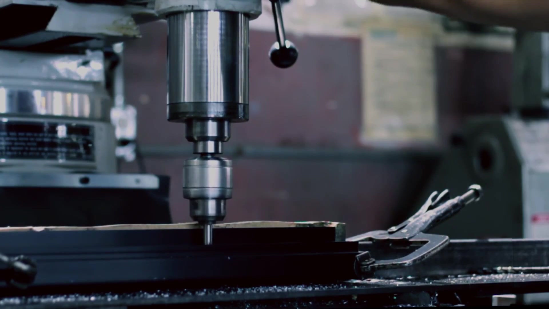
- Laser Machining, LM, Laser Cutting, CO2 Laser Processing, Nd-YAG Cut
Laser Machining - LM - Laser Cutting - Custom Parts Manufacturing - CO2 Laser Processing - Nd-YAG - Cutting - Boring Laser Machining & Cutting & LBM LASER CUTTING is a HIGH-ENERGY-BEAM MANUFACTURING technology that uses a laser to cut materials, and is typically used for industrial manufacturing applications. In LASER BEAM MACHINING (LBM), a laser source focuses optical energy on the surface of the workpiece. Laser cutting directs the highly focused and high-density output of a high-power laser, by computer, at the material to be cut. The targeted material then either melts, burns, vaporizes away, or is blown away by a jet of gas, in a controlled manner leaving an edge with a high-quality surface finish. Our industrial laser cutters are suitable for cutting flat-sheet material as well as structural and piping materials, metallic and nonmetallic workpieces. Generally no vacuum is required in the laser beam machining and cutting processes. There are several types of lasers used in laser cutting and manufacturing. The pulsed or continuous wave CO2 LASER is suited for cutting, boring, and engraving. The NEODYMIUM (Nd) and neodymium yttrium-aluminum-garnet (Nd-YAG) LASERS are identical in style and differ only in application. The neodymium Nd is used for boring and where high energy but low repetition is required. The Nd-YAG laser on the other hand is used where very high power is required and for boring and engraving. Both CO2 and Nd/ Nd-YAG lasers can be used for LASER WELDING. Other lasers we use in manufacturing include Nd:GLASS, RUBY and EXCIMER. In Laser Beam Machining (LBM), the following parameters are important: The reflectivity and thermal conductivity of the workpiece surface and its specific heat and latent heat of melting and evaporation. The efficiency of the Laser Beam Machining (LBM) process increases with decreasing of these parameters. The cutting depth can be expressed as: t ~ P / (v x d) This means, the cutting depth “t” is proportional to the power input P and inversely proportional to cutting speed v and laser-beam spot diameter d. The surface produced with LBM is generally rough and has a heat-affected zone. CARBONDIOXIDE (CO2) LASER CUTTING and MACHINING: The DC-excited CO2 lasers get pumped by passing a current through the gas mix whereas the RF-excited CO2 lasers use radio frequency energy for excitation. The RF method is relatively new and has become more popular. DC designs require electrodes inside the cavity, and therefore they can have electrode erosion and plating of electrode material on the optics. To the contrary, RF resonators have external electrodes and therefore they are not prone to those problems. We use CO2 lasers in industrial cutting of many materials such as mild steel, aluminum, stainless steel, titanium and plastics. YAG LASER CUTTING and MACHINING: We use YAG lasers for cutting and scribing metals and ceramics. The laser generator and external optics require cooling. Waste heat is generated and transferred by a coolant or directly to air. Water is a common coolant, usually circulated through a chiller or heat transfer system. EXCIMER LASER CUTTING and MACHINING: An excimer laser is a kind of laser with wavelengths in the ultraviolet region. The exact wavelength depends on the molecules used. For example the following wavelengths are associated with the molecules shown in parantheses: 193 nm (ArF), 248 nm (KrF), 308 nm (XeCl), 353 nm (XeF). Some excimer lasers are tunable. Excimer lasers have the attractive property that they can remove very fine layers of surface material with almost no heating or change to the remainder of the material. Therefore excimer lasers are well suited to precision micromachining of organic materials such as some polymers and plastics. GAS-ASSISTED LASER CUTTING: Sometimes we use laser beams in combination with a gas stream, like oxygen, nitrogen or argon for cutting thin sheet materials. This is done using a LASER-BEAM TORCH. For stainless steel and aluminum we use high-pressure inert-gas-assisted laser cutting using nitrogen. This results in oxide-free edges to improve weldability. These gas streams also blow away molten and vaporized material from workpiece surfaces. In a LASER MICROJET CUTTING we have a water-jet guided laser in which a pulsed laser beam is coupled into a low-pressure water jet. We use it to perform laser cutting while using the water jet to guide the laser beam, similar to an optical fiber. The advantages of laser microjet are that the water also removes debris and cools the material, it is faster than traditional ''dry'' laser cutting with higher dicing speeds, parallel kerf and omnidirectional cutting capability. We deploy different methods in cutting using lasers. Some of the methods are vaporization, melt and blow, melt blow and burn, thermal stress cracking, scribing, cold cutting and burning, stabilized laser cutting. - Vaporization cutting: The focused beam heats the surface of the material to its boiling point and creates a hole. The hole leads to a sudden increase in absorptivity and quickly deepens the hole. As the hole deepens and the material boils, the generated vapor erodes the molten walls blowing material out and further enlarging the hole. Non melting material such as wood, carbon and thermoset plastics are usually cut by this method. - Melt and blow cutting: We use high-pressure gas to blow molten material from the cutting area, decreasing the required power. The material is heated to its melting point and then a gas jet blows the molten material out of the kerf. This eliminates the need to raise the temperature of the material any further. We cut metals with this technique. - Thermal stress cracking: Brittle materials are sensitive to thermal fracture. A beam is focused on the surface causing localized heating and thermal expansion. This results in a crack that can then be guided by moving the beam. We use this technique in glass cutting. - Stealth dicing of silicon wafers: The separation of microelectronic chips from silicon wafers is performed by the stealth dicing process, using a pulsed Nd:YAG laser, the wavelength of 1064 nm is well adopted to the electronic band gap of silicon (1.11 eV or 1117 nm). This is popular in semiconductor device fabrication. - Reactive cutting: Also called flame cutting, this technique can be resembled to oxygen torch cutting but with a laser beam as the ignition source. We use this for cutting carbon steel in thicknesses over 1 mm and even very thick steel plates with little laser power. PULSED LASERS provide us a high-power burst of energy for a short period and are very effective in some laser cutting processes, such as piercing, or when very small holes or very low cutting speeds are required. If a constant laser beam was used instead, the heat could reach the point of melting the entire piece being machined. Our lasers have the ability to pulse or cut CW (Continuous Wave) under NC (numerical control) program control. We use DOUBLE PULSE LASERS emitting a series of pulse pairs to improve material removal rate and hole quality. The first pulse removes material from the surface and the second pulse prevents the ejected material from readhering to the side of the hole or cut. Tolerances and surface finish in laser cutting and machining are outstanding. Our modern laser cutters have positioning accuracies in the neighborhood of 10 micrometers and repeatabilities of 5 micrometers. Standard roughnesses Rz increase with the sheet thickness, but decreases with laser power and cutting speed. The laser cutting and machining processes are capable of achieving close tolerances, often to within 0.001 inch (0.025 mm) Part geometry and the mechanical features of our machines are optimized to achieve best tolerance capabilities. Surface finishes we can obtain from laser beam cutting may range between 0.003 mm to 0.006 mm. Generally we easily achieve holes with 0.025 mm diameter, and holes as small as 0.005 mm and hole depth-to-diameter ratios of 50 to 1 have been produced in various materials. Our simplest and most standard laser cutters will cut carbon steel metal from 0.020–0.5 inch (0.51–13 mm) in thickness and can easily be up to thirty times faster than standard sawing. Laser-beam machining is used widely for drilling and cutting of metals, nonmetals and composite materials. Advantages of laser cutting over mechanical cutting include easier workholding, cleanliness and reduced contamination of the workpiece (since there is no cutting edge as in traditional milling or turning which can become contaminated by the material or contaminate the material, i.e. bue build-up). The abrasive nature of composite materials may make them difficult to machine by conventional methods but easy by laser machining. Because the laser beam does not wear during the process, precision obtained may be better. Because laser systems have a small heat-affected zone, there is also a lesser chance of warping the material that is being cut. For some materials laser cutting can be the only option. Laser-beam cutting processes are flexible, and fiber optic beam delivery, simple fixturing, short set-up times, availability of three dimensional CNC systems make it possible for laser cutting and machining to compete successfully with other sheet metal fabrication processes such as punching. This being said, laser technology can sometimes be combined with the mechanical fabrication technologies for improved overall efficiency. Laser cutting of sheet metals has the advantages over plasma cutting of being more precise and using less energy, however, most industrial lasers cannot cut through the greater metal thickness that plasma can. Lasers operating at higher powers such as 6000 Watts are approaching plasma machines in their ability to cut through thick materials. However the capital cost of these 6000 Watt laser cutters is much higher than that of plasma cutting machines capable of cutting thick materials like steel plate. There are also disadvantages of laser cutting and machining. Laser cutting involves high power consumption. Industrial laser efficiencies may range from 5% to 15%. The power consumption and efficiency of any particular laser will vary depending on output power and operating parameters. This will depend on type of laser and how well the laser matches the work at hand. Amount of laser cutting power required for a particular task depends on the material type, thickness, process (reactive/inert) used and the desired cutting rate. The maximum production rate in laser cutting and machining is limited by a number of factors including laser power, process type (whether reactive or inert), material properties and thickness. In LASER ABLATION we remove material from a solid surface by irradiating it with a laser beam. At low laser flux, the material is heated by the absorbed laser energy and evaporates or sublimates. At high laser flux, the material is typically converted to a plasma. High power lasers clean a large spot with a single pulse. Lower power lasers use many small pulses which may be scanned across an area. In laser ablation we remove material with a pulsed laser or with a continuous wave laser beam if the laser intensity is high enough. Pulsed lasers can drill extremely small, deep holes through very hard materials. Very short laser pulses remove material so quickly that the surrounding material absorbs very little heat, therefore laser drilling can be done on delicate or heat-sensitive materials. Laser energy can be selectively absorbed by coatings, therefore CO2 and Nd:YAG pulsed lasers can be used to clean surfaces, remove paint and coating, or prepare surfaces for painting without damaging the underlying surface. We use LASER ENGRAVING and LASER MARKING to engrave or mark an object. These two techniques are in fact the most widely used applications. No inks are used, nor does it involve tool bits which contact the engraved surface and wear out which is the case with traditional mechanical engraving and marking methods. Materials specially designed for laser engraving and marking include laser-sensitive polymers and special new metal alloys. Although laser marking and engraving equipment is relatively more expensive compared to alternatives such as punches, pins, styli, etching stamps….etc., they have become more popular due to their accuracy, reproducibility, flexibility, ease of automation and on-line application in a wide variety of manufacturing environments. Finally, we use laser beams for several other manufacturing operations: - LASER WELDING - LASER HEAT TREATING: Small-scale heat treating of metals and ceramics to modify their surface mechanical and tribological properties. - LASER SURFACE TREATMENT / MODIFICATION: Lasers are used to clean surfaces, introduce functional groups, modify surfaces in an effort to improve adhesion prior to coating deposition or joining processes. CLICK Product Finder-Locator Service RÛPERA BERÊ
- Fiber Optic Components, Splicing Enclosures, FTTH Node, CATV Products
Fiber Optic Components - Splicing Enclosures - FTTH Node - Fiber Distribution Box - Optical Platform - CATV Products - Telecommunication Optics - AGS-TECH Inc. Berhemên Fiber Optîk We supply: • Fiber optic connectors, adapters, terminators, pigtails, patchcords, connector faceplates, shelves, communication racks, fiber distribution box, splicing enclosure, FTTH node, optical platform, fiber optic taps, splitters-combiners, fixed and variable optical attenuators, optical switch, DWDM, MUX/DEMUX, EDFA, Raman amplifiers and other amplifiers, isolator, circulator, gain flattener, custom fiberoptic assembly for telecommunication systems, optical waveguide devices, CATV products • Lasers and photodetectors, PSD (Position Sensitive Detectors), quadcells • Fiber optic assemblies for industrial applications (illumination, light delivery or inspection of pipe interiors, crevices, cavities, body interiors....). • Fiberoptic assemblies for medical applications (see our site http://www.agsmedical.com for medical endoscopes and couplers). Among the products our engineers have developed is a super slim 0.6 mm diameter flexible video endoscope, and a fiber end inspection interferometer. The interferometer was developed by our engineers for in-process and final inspection in manufacturing of fiber connectors. We use special bonding and attachment techniques and materials for rigid, reliable and long life assemblies. Even under extensive environmental cycling such as high temperature/low temperature; high humidity/low humidity our assemblies remain intact and keep working. Download our catalog for passive fiber optic components Download our catalog for active fiber optic products Download our catalog for free space optical components and assemblies Private Label Medical Endoscopes and Visualization Systems (We can put your company name and logo on these) CLICK Product Finder-Locator Service RÛPERA BERÊ
- Electrochemical Machining and Grinding - ECM - Reverse Electroplating
Electrochemical Machining and Grinding - ECM - Reverse Electroplating - Custom Machining - AGS-TECH Inc. - NM - USA ECM Machining, Machining Electrochemical, Grinding Some of the valuable NON-CONVENTIONAL MANUFACTURING processes AGS-TECH Inc offers are ELECTROCHEMICAL MACHINING (ECM), SHAPED-TUBE ELECTROLYTIC MACHINING (STEM), PULSED ELECTROCHEMICAL MACHINING (PECM), ELECTROCHEMICAL GRINDING (ECG), HYBRID MACHINING PROCESSES. ELECTROCHEMICAL MACHINING (ECM) is a non-conventional manufacturing technique where metal is removed by an electrochemical process. ECM is typically a mass production technique, used for machining extremely hard materials and materials that are difficult to machine using the conventional manufacturing methods. Electrochemical-machining systems we use for production are numerically controlled machining centers with high production rates, flexibility, perfect control of dimensional tolerances. Electrochemical machining is capable of cutting small and odd-shaped angles, intricate contours or cavities in hard and exotic metals like titanium aluminides, Inconel, Waspaloy, and high nickel, cobalt, and rhenium alloys. Both external and internal geometries can be machined. Modifications of the electrochemical machining process are used for operations like turning, facing, slotting, trepanning, profiling where the electrode becomes the cutting tool. The metal removal rate is only a function of ion exchange rate and is not affected by the strength, hardness or toughness of the workpiece. Unfortunately the method of electrochemical machining (ECM) is limited to electrically conductive materials. Another important point to consider deploying the ECM technique is to compare the mechanical properties of the produced parts with those produced by other machining methods. ECM removes material instead of adding it and therefore is sometimes referred to as ''reverse electroplating''. It resembles in some ways to electrical discharge machining (EDM) in that a high current is passed between an electrode and the part, through an electrolytic material removal process having a negatively charged electrode (cathode), a conductive fluid (electrolyte), and a conductive workpiece (anode). The electrolyte acts as the current carrier and is a highly conductive inorganic salt solution like sodium chloride mixed and dissolved in water or sodium nitrate. The advantage of ECM is that there is no tool wear. The ECM cutting tool is guided along the desired path close to the work but without touching the piece. Unlike EDM, however, no sparks are created. High metal removal rates and mirror surface finishes are possible with ECM, with no thermal or mechanical stresses being transferred to the part. ECM does not cause any thermal damage to the part and since there are no tool forces there is no distortion to the part and no tool wear, as would be the case with typical machining operations. In electrochemical machining cavity produced is the female mating image of the tool. In the ECM process, a cathode tool is moved into an anode workpiece. The shaped tool is generally made of copper, brass, bronze or stainless steel. The pressurized electrolyte is pumped at a high rate at a set temperature through the passages in the tool to the area being cut. The feed rate is the same as the rate of ''liquification'' of the material, and the electrolyte movement in the tool-workpiece gap washes metal ions away from the workpiece anode before they have a chance to plate onto the cathode tool. The gap between the tool and the workpiece varies between 80-800 micrometers and the DC power supply in the range 5 – 25 V maintains current densities between 1.5 – 8 A/mm2 of active machined surface. As electrons cross the gap, material from the workpiece is dissolved, as the tool forms the desired shape in the workpiece. The electrolytic fluid carries away the metal hydroxide formed during this process. Commercial electrochemical machines with current capacities between 5A and 40,000A are available. The material removal rate in electrochemical machining can be expressed as: MRR = C x I x n Here MRR=mm3/min, I=current in amperes, n=current efficiency, C=a material constant in mm3/A-min. The constant C depends on valence for pure materials. The higher the valence, the lower is its value. For most metals it is in between 1 and 2. If Ao denotes the uniform cross-sectional area being electrochemically machined in mm2, the feed rate f in mm/min can be expressed as: F = MRR / Ao Feed rate f is the speed the electrode is penetrating the workpiece. In the past there were problems of poor dimensional accuracy and environmentally polluting waste from electrochemical machining operations. These have largely been overcome. Some of the applications of electrochemical machining of high-strength materials are: - Die-Sinking operations. Die-sinking is machining forging – die cavities. - Drilling a jet engine turbine blades, jet-engine parts and nozzles. - Multiple small holes drilling. The electrochemical machining process leaves a burr-free surface. - Steam turbine blades can be machined within close limits. - For deburring of surfaces. In deburring, ECM removes metal projections left from the machining processes and so dulls sharp edges. Electrochemical machining process is fast and often more convenient than the conventional methods of deburring by hand or non-traditional machining processes. SHAPED-TUBE ELECTROLYTIC MACHINING (STEM) is a version of electrochemical machining process we use for drilling small diameter deep holes. A titanium tube is used as the tool which is coated with an electrically insulating resin to prevent the removal of material from other regions like the lateral faces of the hole and tube. We can drill hole sizes of 0.5 mm with depth-to-diameter ratios of 300:1 PULSED ELECTROCHEMICAL MACHINING (PECM): We use very high pulsed current densities in the order of 100 A/cm2. By using pulsed currents we eliminate the need for high electrolyte flow rates which poses limitations for the ECM method in mold and die fabrication. Pulsed electrochemical machining improves fatigue life and eliminates the recast layer left by the electrical discharge machining (EDM) technique on mold and die surfaces. In ELECTROCHEMICAL GRINDING (ECG) we combine the conventional grinding operation with electrochemical machining. The grinding wheel is a rotating cathode with abrasive particles of diamond or aluminum oxide that are metal bonded. The current densities range between 1 and 3 A/mm2. Similar to ECM, an electrolyte such as sodium nitrate flows and the metal removal in electrochemical grinding is dominated by the electrolytic action. Less than 5% of metal removal is by abrasive action of the wheel. The ECG technique is well suited for carbides and high-strength alloys, but not so much of a fit for die-sinking or mould making because the grinder may not easily access deep cavities. The material removal rate in electrochemical grinding can be expressed as: MRR = G I / d F Here MRR is in mm3/min, G is mass in grams, I is current in amperes, d is density in g/mm3 and F is Faraday’s constant (96,485 Coulombs/mole). The speed of penetration of the grinding wheel into workpiece can be expressed as: Vs = (G / d F) x (E / g Kp) x K Here Vs is in mm3/min, E is cell voltage in volts, g is wheel to workpiece gap in mm, Kp is coefficient of loss and K is electrolyte conductivity. The advantage of the electrochemical grinding method over conventional grinding is less wheel wear because less than 5% of the metal removal is by abrasive action of the wheel. There are similarities between EDM and ECM: 1. The tool and workpiece are separated by a very small gap without a contact in between them. 2. Both tool and material must be conductors of electricity. 3. Both techniques need high capital investment. Modern CNC machines are used 4. Both methods consume lots of electric power. 5. A conductive fluid is used as a medium between the tool and the work piece for ECM and a dielectric fluid for EDM. 6. The tool is fed continuously towards the workpiece to maintain a constant gap between them (EDM may incorporate intermittent or cyclic, typically partial, tool withdrawal). HYBRID MACHINING PROCESSES: We frequently take advantage of the benefits of hybrid machining processes where two or more different processes such as ECM, EDM….etc. are used in combination. This gives us the opportunity to overcome the shortcomings of one process by the other, and benefit from the advantages of each process. CLICK Product Finder-Locator Service RÛPERA BERÊ
- Electronic Testers, Electrical Properties Testing, Oscilloscope, Pulse
Electronic Testers - Electrical Test Equipment - Electrical Properties Testing - Oscilloscope - Signal Generator - Function Generator - Pulse Generator - Frequency Synthesizer - Multimeter Amûrên Testê yên Elektrîkî û Elektronîkî With the term ELECTRONIC TESTER we refer to test equipment that is used primarily for testing, inspection and analysis of electrical and electronic components and systems. We offer the most popular ones in the industry: POWER SUPPLIES & SIGNAL GENERATING DEVICES: POWER SUPPLY, SIGNAL GENERATOR, FREQUENCY SYNTHESIZER, FUNCTION GENERATOR, DIGITAL PATTERN GENERATOR, PULSE GENERATOR, SIGNAL INJECTOR METERS: DIGITAL MULTIMETERS, LCR METER, EMF METER, CAPACITANCE METER, BRIDGE INSTRUMENT, CLAMP METER, GAUSSMETER / TESLAMETER/ MAGNETOMETER, GROUND RESISTANCE METER ANALYZERS: OSCILLOSCOPES, LOGIC ANALYZER, SPECTRUM ANALYZER, PROTOCOL ANALYZER, VECTOR SIGNAL ANALYZER, TIME-DOMAIN REFLECTOMETER, SEMICONDUCTOR CURVE TRACER, NETWORK ANALYZER, PHASE ROTATION TESTER, FREQUENCY COUNTER You can purchase brand new, refurbished or used test equipment from us at the most competitive discounted prices. Simply choose the product from the downloadable catalogs and let us know the product name, product code and relevant information and we will send you our quote. Download by clicking on highlighted text: ANRITSU Electronic Measuring Instruments FLUKE Test Tools Catalog KEYSIGHT Basic Automotive Test Products KEYSIGHT Basic Instruments KEYSIGHT Bench and Power Products KEYSIGHT Network Analyzer Products KEYSIGHT Signal Generation Solutions KEYSIGHT Smart Bench Essentials Series Products KEYSIGHT High-Volume Traffic Generator Products KEYSIGHT Layer 4-7 Network Test Products KEYSIGHT Layer 2-3 Network Test Products KEYSIGHT Distribution Products Catalog MEGGER Low Voltage Test Tools Catalog MICROWAVE Flexible Cable Assembly MICROWAVE and MILIMETER WAVE Test Accessories Brochure (Cable assemblies, VNA Test Assemblies, Mechanical Calibration Kits, RF Coaxial Adapters, Test Port Adapters, DC Blocks, NMD Connectors....etc.) Private Label Hand Tools for Every Industry (This catalog contains a few electrical & electronic test instruments. We can private label these hand tools if you wish. In other words, we can put your company name, brand and label on them. This way you can promote your brand by reselling these to your customers.) ROHDE SCHWARZ Benchtop Power Supplies Ideal for labs and system racks, galvanic isolation, floating channels, constant voltage or current modes, protection functions, parallel and serial operation, low ripple/noise, remote sensing option ROHDE SCHWARZ Test Equipment Catalog (Oscilloscopes, Power Supplies, Signal Generators, Handheld Analyzers, Spectrum Analyzers, Vector Network Analyzers, Meters & Counters) TEKTRONIX Product Catalog for Test and Measurement Solutions VANDAL-PROOF IP65/IP67/IP68 Keyboards, Keypads, Pointing Devices, ATM Pinpads, Medical & Military Keyboards and other similar Rugged Computer Peripherals For details and other similar equipment, please visit our equipment website: http://www.sourceindustrialsupply.com Let us briefly go over some of these equipment in everyday use throughout the industry: The electrical power supplies we supply for metrology purposes are discrete, benchtop and stand-alone devices. The ADJUSTABLE REGULATED ELECTRICAL POWER SUPPLIES are some of the most popular ones, because their output values can be adjusted and their output voltage or current is maintained constant even if there are variations in input voltage or load current. ISOLATED POWER SUPPLIES have power outputs that are electrically independent of their power inputs. Depending on their power conversion method, there are LINEAR and SWITCHING POWER SUPPLIES. The linear power supplies process the input power directly with all their active power conversion components working in the linear regions, whereas the switching power supplies have components working predominantly in non-linear modes (such as transistors) and convert power to AC or DC pulses before processing. Switching power supplies are generally more efficient than linear supplies because they lose less power due to shorter times their components spend in the linear operating regions. Depending on application, a DC or AC power is used. Other popular devices are PROGRAMMABLE POWER SUPPLIES, where voltage, current or frequency can be remotely controlled through an analog input or digital interface such as an RS232 or GPIB. Many of them have an integral microcomputer to monitor and control the operations. Such instruments are essential for automated testing purposes. Some electronic power supplies use current limiting instead of cutting off power when overloaded. Electronic limiting is commonly used on lab bench type instruments. SIGNAL GENERATORS are another widely used instruments in lab and industry, generating repeating or non-repeating analog or digital signals. Alternatively they are also called FUNCTION GENERATORS, DIGITAL PATTERN GENERATORS or FREQUENCY GENERATORS. Function generators generate simple repetitive waveforms such as sine waves, step pulses, square & triangular and arbitrary waveforms. With Arbitrary waveform generators the user can generate arbitrary waveforms, within published limits of frequency range, accuracy, and output level. Unlike function generators, which are limited to a simple set of waveforms, an arbitrary waveform generator allows the user to specify a source waveform in a variety of different ways. RF and MICROWAVE SIGNAL GENERATORS are used for testing components, receivers and systems in applications such as cellular communications, WiFi, GPS, broadcasting, satellite communications and radars. RF signal generators generally work between a few kHz to 6 GHz, while microwave signal generators operate within a much wider frequency range, from less than 1 MHz to at least 20 GHz and even up to hundreds of GHz ranges using special hardware. RF and microwave signal generators can be classified further as analog or vector signal generators. AUDIO-FREQUENCY SIGNAL GENERATORS generate signals in the audio-frequency range and above. They have electronic lab applications checking of the frequency response of audio equipment. VECTOR SIGNAL GENERATORS, sometimes also referred to as DIGITAL SIGNAL GENERATORS are capable of generating digitally-modulated radio signals. Vector signal generators can generate signals based on industry standards such as GSM, W-CDMA (UMTS) and Wi-Fi (IEEE 802.11). LOGIC SIGNAL GENERATORS are also called DIGITAL PATTERN GENERATOR. These generators produce logic types of signals, that is logic 1s and 0s in the form of conventional voltage levels. Logic signal generators are used as stimulus sources for functional validation & testing of digital integrated circuits and embedded systems. The devices mentioned above are for general-purpose use. There are however many other signal generators designed for custom specific applications. A SIGNAL INJECTOR is a very useful and quick troubleshooting tool for signal tracing in a circuit. Technicians can determine the faulty stage of a device such as a radio receiver very quickly. The signal injector can be applied to the speaker output, and if the signal is audible one can move to the preceding stage of the circuit. In this case an audio amplifier, and if the injected signal is heard again one can move the signal injection up the stages of the circuit until the signal is no longer audible. This will serve the purpose of locating the location of the problem. A MULTIMETER is an electronic measuring instrument combining several measurement functions in one unit. Generally, multimeters measure voltage, current, and resistance. Both digital and analog version are available. We offer portable hand-held multimeter units as well as laboratory-grade models with certified calibration. Modern multimeters can measure many parameters such as: Voltage (both AC / DC), in volts, Current (both AC / DC), in amperes, Resistance in ohms. Additionally, some multimeters measure: Capacitance in farads, Conductance in siemens, Decibels, Duty cycle as a percentage, Frequency in hertz, Inductance in henries, Temperature in degrees Celsius or Fahrenheit, using a temperature test probe. Some multimeters also include: Continuity tester; sounds when a circuit conducts, Diodes (measuring forward drop of diode junctions), Transistors (measuring current gain and other parameters), battery checking function, light level measuring function, acidity & Alkalinity (pH) measuring function and relative humidity measuring function. Modern multimeters are often digital. Modern digital multimeters often have an embedded computer to make them very powerful tools in metrology and testing. They include features such as:: •Auto-ranging, which selects the correct range for the quantity under test so that the most significant digits are shown. •Auto-polarity for direct-current readings, shows if the applied voltage is positive or negative. •Sample and hold, which will latch the most recent reading for examination after the instrument is removed from the circuit under test. •Current-limited tests for voltage drop across semiconductor junctions. Even though not a replacement for a transistor tester, this feature of digital multimeters facilitates testing diodes and transistors. •A bar graph representation of the quantity under test for better visualization of fast changes in measured values. •A low-bandwidth oscilloscope. •Automotive circuit testers with tests for automotive timing and dwell signals. •Data acquisition feature to record maximum and minimum readings over a given period, and to take a number of samples at fixed intervals. •A combined LCR meter. Some multimeters can be interfaced with computers, while some can store measurements and upload them to a computer. Yet another very useful tool, an LCR METER is a metrology instrument for measuring the inductance (L), capacitance (C), and resistance (R) of a component. The impedance is measured internally and converted for display to the corresponding capacitance or inductance value. Readings will be reasonably accurate if the capacitor or inductor under test does not have a significant resistive component of impedance. Advanced LCR meters measure true inductance and capacitance, and also the equivalent series resistance of capacitors and the Q factor of inductive components. The device under test is subjected to an AC voltage source and the meter measures the voltage across and the current through the tested device. From the ratio of voltage to current the meter can determine the impedance. The phase angle between the voltage and current is also measured in some instruments. In combination with the impedance, the equivalent capacitance or inductance, and resistance, of the device tested can be calculated and displayed. LCR meters have selectable test frequencies of 100 Hz, 120 Hz, 1 kHz, 10 kHz, and 100 kHz. Benchtop LCR meters typically have selectable test frequencies of more than 100 kHz. They often include possibilities to superimpose a DC voltage or current on the AC measuring signal. While some meters offer the possibility to externally supply these DC voltages or currents other devices supply them internally. An EMF METER is a test & metrology instrument for measuring electromagnetic fields (EMF). Majority of them measure the electromagnetic radiation flux density (DC fields) or the change in an electromagnetic field over time (AC fields). There are single axis and tri-axis instrument versions. Single axis meters cost less than tri-axis meters, but take longer to complete a test because the meter only measures one dimension of the field. Single axis EMF meters have to be tilted and turned on all three axes to complete a measurement. On the other hand, tri-axis meters measure all three axes simultaneously, but are more expensive. An EMF meter can measure AC electromagnetic fields, which emanate from sources such as electrical wiring, while GAUSSMETERS / TESLAMETERS or MAGNETOMETERS measure DC fields emitted from sources where direct current is present. The majority of EMF meters are calibrated to measure 50 and 60 Hz alternating fields corresponding to the frequency of US and European mains electricity. There are other meters which can measure fields alternating at as low as 20 Hz. EMF measurements can be broadband across a wide range of frequencies or frequency selective monitoring only the frequency range of interest. A CAPACITANCE METER is a test equipment used to measure capacitance of mostly discrete capacitors. Some meters display the capacitance only, whereas others also display leakage, equivalent series resistance, and inductance. Higher end test instruments use techniques such as inserting the capacitor-under-test into a bridge circuit. By varying the values of the other legs in the bridge so as to bring the bridge into balance, the value of the unknown capacitor is determined. This method ensures greater precision. The bridge may also be capable to measure series resistance and inductance. Capacitors over a range from picofarads to farads may be measured. Bridge circuits do not measure leakage current, but a DC bias voltage can be applied and the leakage measured directly. Many BRIDGE INSTRUMENTS can be connected to computers and data exchange be made to download readings or to control the bridge externally. Such bridge instruments aso offer go / no go testing for automation of tests in a fast paced production & quality control environment. Yet, another test instrument, a CLAMP METER is an electrical tester combining a voltmeter with a clamp type current meter. Most modern versions of clamp meters are digital. Modern clamp meters have most of the basic functions of a Digital Multimeter, but with the added feature of a current transformer built into the product. When you clamp the instrument’s “jaws” around a conductor carrying a large ac current, that current is coupled through the jaws, similar to the iron core of a power transformer, and into a secondary winding which is connected across the shunt of the meter’s input, the principle of operation resembling much that of a transformer. A much smaller current is delivered to the meter’s input due to the ratio of the number of secondary windings to the number of primary windings wrapped around the core. The primary is represented by the one conductor around which the jaws are clamped. If the secondary has 1000 windings, then the secondary current is 1/1000 the current flowing in the primary, or in this case the conductor being measured. Thus, 1 amp of current in the conductor being measured would produce 0.001 amps of current at the input of the meter. With clamp meters much larger currents can be easily measured by increasing the number of turns in the secondary winding. As with most of our test equipment, advanced clamp meters offer logging capability. GROUND RESISTANCE TESTERS are used for testing the earth electrodes and the soil resistivity. The instrument requirements depend on the range of applications. Modern clamp-on ground testing instruments simplify ground loop testing and enable non-intrusive leakage current measurements. Among the ANALYZERS we sell are OSCILLOSCOPES without doubt one of the most widely used equipment. An oscilloscope, also called an OSCILLOGRAPH, is a type of electronic test instrument that allows observation of constantly varying signal voltages as a two-dimensional plot of one or more signals as a function of time. Non-electrical signals like sound and vibration can also be converted to voltages and displayed on oscilloscopes. Oscilloscopes are used to observe the change of an electrical signal over time, the voltage and time describe a shape which is continuously graphed against a calibrated scale. Observation and analysis of the waveform reveals us properties such as amplitude, frequency, time interval, rise time, and distortion. Oscilloscopes can be adjusted so that repetitive signals can be observed as a continuous shape on the screen. Many oscilloscopes have storage function that allows single events to be captured by the instrument and displayed for a relatively long time. This allows us to observe events too fast to be directly perceptible. Modern oscilloscopes are lightweight, compact and portable instruments. There are also miniature battery-powered instruments for field service applications. Laboratory grade oscilloscopes are generally bench-top devices. There is a vast variety of probes and input cables for use with oscilloscopes. Please contact us in case you need advice about which one to use in your application. Oscilloscopes with two vertical inputs are called dual-trace oscilloscopes. Using a single-beam CRT, they multiplex the inputs, usually switching between them fast enough to display two traces apparently at once. There are also oscilloscopes with more traces; four inputs are common among these. Some multi-trace oscilloscopes use the external trigger input as an optional vertical input, and some have third and fourth channels with only minimal controls. Modern oscilloscopes have several inputs for voltages, and thus can be used to plot one varying voltage versus another. This is used for example for graphing I-V curves (current versus voltage characteristics) for components such as diodes. For high frequencies and with fast digital signals the bandwidth of the vertical amplifiers and sampling rate must be high enough. For-general purpose use a bandwidth of at least 100 MHz is usually sufficient. A much lower bandwidth is sufficient for audio-frequency applications only. Useful range of sweeping is from one second to 100 nanoseconds, with appropriate triggering and sweep delay. A well-designed, stable, trigger circuit is required for a steady display. The quality of the trigger circuit is key for good oscilloscopes. Another key selection criteria is the sample memory depth and sample rate. Basic level modern DSOs now have 1MB or more of sample memory per channel. Often this sample memory is shared between channels, and can sometimes only be fully available at lower sample rates. At the highest sample rates the memory may be limited to a few 10's of KB. Any modern ''real-time'' sample rate DSO will have typically 5-10 times the input bandwidth in sample rate. So a 100 MHz bandwidth DSO would have 500 Ms/s - 1 Gs/s sample rate. Greatly increased sample rates have largely eliminated the display of incorrect signals that was sometimes present in the first generation of digital scopes. Most modern oscilloscopes provide one or more external interfaces or buses such as GPIB, Ethernet, serial port, and USB to allow remote instrument control by external software. Here is a list of different oscilloscope types: CATHODE RAY OSCILLOSCOPE DUAL-BEAM OSCILLOSCOPE ANALOG STORAGE OSCILLOSCOPE DIGITAL OSCILLOSCOPES MIXED-SIGNAL OSCILLOSCOPES HANDHELD OSCILLOSCOPES PC-BASED OSCILLOSCOPES A LOGIC ANALYZER is an instrument that captures and displays multiple signals from a digital system or digital circuit. A logic analyzer may convert the captured data into timing diagrams, protocol decodes, state machine traces, assembly language. Logic Analyzers have advanced triggering capabilities, and are useful when the user needs to see the timing relationships between many signals in a digital system. MODULAR LOGIC ANALYZERS consist of both a chassis or mainframe and logic analyzer modules. The chassis or mainframe contains the display, controls, control computer, and multiple slots into which the data-capturing hardware is installed. Each module has a specific number of channels, and multiple modules can be combined to obtain a very high channel count. The ability to combine multiple modules to obtain a high channel count and the generally higher performance of modular logic analyzers makes them more expensive. For the very high end modular logic analyzers, the users may need to provide their own host PC or purchase an embedded controller compatible with the system. PORTABLE LOGIC ANALYZERS integrate everything into a single package, with options installed at the factory. They generally have lower performance than modular ones, but are economical metrology tools for general purpose debugging. In PC-BASED LOGIC ANALYZERS, the hardware connects to a computer through a USB or Ethernet connection and relays the captured signals to the software on the computer. These devices are generally much smaller and less expensive because they make use of a personal computer’s existing keyboard, display and CPU. Logic analyzers can be triggered on a complicated sequence of digital events, then capture large amounts of digital data from the systems under test. Today specialized connectors are in use. The evolution of logic analyzer probes has led to a common footprint that multiple vendors support, which provides added freedom to end users: Connectorless technology offered as several vendor-specific trade names such as Compression Probing; Soft Touch; D-Max is being used. These probes provide a durable, reliable mechanical and electrical connection between the probe and the circuit board. A SPECTRUM ANALYZER measures the magnitude of an input signal versus frequency within the full frequency range of the instrument. The primary use is to measure the power of the spectrum of signals. There are optical and acoustical spectrum analyzers as well, but here we will discuss only electronic analyzers that measure and analyze electrical input signals. The spectra obtained from electrical signals provides us information about frequency, power, harmonics, bandwidth…etc. The frequency is displayed on the horizonal axis and the signal amplitude on the vertical. Spectrum analyzers are widely used in the electronics industry for the analyses of the frequency spectrum of radio frequency, RF and audio signals. Looking at the spectrum of a signal we are able to reveal elements of the signal, and the performance of the circuit producing them. Spectrum analyzers are able to make a large variety of measurements. Looking at the methods used to obtain the spectrum of a signal we can categorize the spectrum analyzer types. - A SWEPT-TUNED SPECTRUM ANALYZER uses a superheterodyne receiver to down-convert a portion of the input signal spectrum (using a voltage-controlled oscillator and a mixer) to the center frequency of a band-pass filter. With a superheterodyne architecture, the voltage-controlled oscillator is swept through a range of frequencies, taking advantage of the full frequency range of the instrument. Swept-tuned spectrum analyzers are descended from radio receivers. Therefore swept-tuned analyzers are either tuned-filter analyzers (analogous to a TRF radio) or superheterodyne analyzers. In fact, in their simplest form, you could think of a swept-tuned spectrum analyzer as a frequency-selective voltmeter with a frequency range that is tuned (swept) automatically. It is essentially a frequency-selective, peak-responding voltmeter calibrated to display the rms value of a sine wave. The spectrum analyzer can show the individual frequency components that make up a complex signal. However it does not provide phase information, only magnitude information. Modern swept-tuned analyzers (superheterodyne analyzers, in particular) are precision devices that can make a wide variety of measurements. However, they are primarily used to measure steady-state, or repetitive, signals because they can't evaluate all frequencies in a given span simultaneously. The ability to evaluate all frequencies simultaneously is possible with only the real-time analyzers. - REAL-TIME SPECTRUM ANALYZERS: A FFT SPECTRUM ANALYZER computes the discrete Fourier transform (DFT), a mathematical process that transforms a waveform into the components of its frequency spectrum, of the input signal. The Fourier or FFT spectrum analyzer is another real-time spectrum analyzer implementation. The Fourier analyzer uses digital signal processing to sample the input signal and convert it to the frequency domain. This conversion is done using the Fast Fourier Transform (FFT). The FFT is an implementation of the Discrete Fourier Transform, the math algorithm used for transforming data from the time domain to the frequency domain. Another type of real-time spectrum analyzers, namely the PARALLEL FILTER ANALYZERS combine several bandpass filters, each with a different bandpass frequency. Each filter remains connected to the input at all times. After an initial settling time, the parallel-filter analyzer can instantaneously detect and display all signals within the analyzer's measurement range. Therefore, the parallel-filter analyzer provides real-time signal analysis. Parallel-filter analyzer is fast, it measures transient and time-variant signals. However, the frequency resolution of a parallel-filter analyzer is much lower than most swept-tuned analyzers, because the resolution is determined by the width of the bandpass filters. To get fine resolution over a large frequency range, you would need many many individual filters, making it costly and complex. This is why most parallel-filter analyzers, except the simplest ones in the market are expensive. - VECTOR SIGNAL ANALYSIS (VSA) : In the past, swept-tuned and superheterodyne spectrum analyzers covered wide frequency ranges from audio, thru microwave, to millimeter frequencies. In addition, digital signal processing (DSP) intensive fast Fourier transform (FFT) analyzers provided high-resolution spectrum and network analysis, but were limited to low frequencies due to the limits of analog-to-digital conversion and signal processing technologies. Today's wide-bandwidth, vector-modulated, time-varying signals benefit greatly from the capabilities of FFT analysis and other DSP techniques. Vector signal analyzers combine superheterodyne technology with high speed ADC's and other DSP technologies to offer fast high-resolution spectrum measurements, demodulation, and advanced time-domain analysis. The VSA is especially useful for characterizing complex signals such as burst, transient, or modulated signals used in communications, video, broadcast, sonar and ultrasound imaging applications. According to form factors, spectrum analyzers are grouped as benchtop, portable, handheld and networked. Benchtop models are useful for applications where the spectrum analyzer can be plugged into AC power,such as in a lab environment or manufacturing area. Bench top spectrum analyzers generally offer better performance and specifications than the portable or handheld versions. However they are generally heavier and have several fans for cooling. Some BENCHTOP SPECTRUM ANALYZERS offer optional battery packs, allowing them to be used away from a mains outlet. Those are referred to as a PORTABLE SPECTRUM ANALYZERS. Portable models are useful for applications where the spectrum analyzer needs to be taken outside to make measurements or carried while in use. A good portable spectrum analyzer is expected to offer optional battery-powered operation to allow the user to work in places without power outlets, a clearly viewable display to allow the screen to be read in bright sunlight, darkness or dusty conditions, light weight. HANDHELD SPECTRUM ANALYZERS are useful for applications where the spectrum analyzer needs to be very light and small. Handheld analyzers offer a limited capability as compared to larger systems. Advantages of handheld spectrum analyzers are however their very low power consumption, battery-powered operation while in the field to allow the user to move freely outside, very small size & light weight. Finally, NETWORKED SPECTRUM ANALYZERS do not include a display and they are designed to enable a new class of geographically-distributed spectrum monitoring and analysis applications. The key attribute is the ability to connect the analyzer to a network and monitor such devices across a network. While many spectrum analyzers have an Ethernet port for control, they typically lack efficient data transfer mechanisms and are too bulky and/or expensive to be deployed in such a distributed manner. The distributed nature of such devices enable geo-location of transmitters, spectrum monitoring for dynamic spectrum access and many other such applications. These devices are able to synchronize data captures across a network of analyzers and enable Network-efficient data transfer for a low cost. A PROTOCOL ANALYZER is a tool incorporating hardware and/or software used to capture and analyze signals and data traffic over a communication channel. Protocol analyzers are mostly used for measuring performance and troubleshooting. They connect to the network to calculate key performance indicators to monitor the network and speed-up troubleshooting activities. A NETWORK PROTOCOL ANALYZER is a vital part of a network administrator's toolkit. Network protocol analysis is used to monitor the health of network communications. To find out why a network device is functioning in a certain way, administrators use a protocol analyzer to sniff the traffic and expose the data and protocols that pass along the wire. Network protocol analyzers are used to - Troubleshoot hard-to-solve problems - Detect and identify malicious software / malware. Work with an Intrusion Detection System or a honeypot. - Gather information, such as baseline traffic patterns and network-utilization metrics - Identify unused protocols so that you can remove them from the network - Generate traffic for penetration testing - Eavesdrop on traffic (e.g., locate unauthorized Instant Messaging traffic or wireless Access Points) A TIME-DOMAIN REFLECTOMETER (TDR) is an instrument that uses time-domain reflectometry to characterize and locate faults in metallic cables such as twisted pair wires and coaxial cables, connectors, printed circuit boards,….etc. Time-Domain Reflectometers measure reflections along a conductor. In order to measure them, the TDR transmits an incident signal onto the conductor and looks at its reflections. If the conductor is of a uniform impedance and is properly terminated, then there will be no reflections and the remaining incident signal will be absorbed at the far end by the termination. However, if there is an impedance variation somewhere, then some of the incident signal will be reflected back to the source. The reflections will have the same shape as the incident signal, but their sign and magnitude depend on the change in impedance level. If there is a step increase in the impedance, then the reflection will have the same sign as the incident signal and if there is a step decrease in impedance, the reflection will have the opposite sign. The reflections are measured at the output/input of the Time-Domain Reflectometer and displayed as a function of time. Alternatively, the display can show the transmission and reflections as a function of cable length because the speed of signal propagation is almost constant for a given transmission medium. TDRs can be used to analyze cable impedances and lengths, connector and splice losses and locations. TDR impedance measurements provide designers the opportunity to perform signal integrity analysis of system interconnects and accurately predict the digital system performance. TDR measurements are widely used in board characterization work. A circuit board designer can determine the characteristic impedances of board traces, compute accurate models for board components, and predict board performance more accurately. There are many other areas of application for time-domain reflectometers. A SEMICONDUCTOR CURVE TRACER is a test equipment used to analyze the characteristics of discrete semiconductor devices such as diodes, transistors, and thyristors. The instrument is based on oscilloscope, but contains also voltage and current sources that can be used to stimulate the device under test. A swept voltage is applied to two terminals of the device under test, and the amount of current that the device permits to flow at each voltage is measured. A graph called V-I (voltage versus current) is displayed on the oscilloscope screen. Configuration includes the maximum voltage applied, the polarity of the voltage applied (including the automatic application of both positive and negative polarities), and the resistance inserted in series with the device. For two terminal devices like diodes, this is sufficient to fully characterize the device. The curve tracer can display all of the interesting parameters such as the diode's forward voltage, reverse leakage current, reverse breakdown voltage,…etc. Three-terminal devices such as transistors and FETs also use a connection to the control terminal of the device being tested such as the Base or Gate terminal. For transistors and other current based devices, the base or other control terminal current is stepped. For field effect transistors (FETs), a stepped voltage is used instead of a stepped current. By sweeping the voltage through the configured range of main terminal voltages, for each voltage step of the control signal, a group of V-I curves is generated automatically. This group of curves makes it very easy to determine the gain of a transistor, or the trigger voltage of a thyristor or TRIAC. Modern semiconductor curve tracers offer many attractive features such as intuitive Windows based user interfaces, I-V, C-V and pulse generation, and pulse I-V, application libraries included for every technology…etc. PHASE ROTATION TESTER / INDICATOR: These are compact and rugged test instruments to identify phase sequence on three-phase systems and open/de-energized phases. They are ideal for installing rotating machinery, motors and for checking generator output. Among the applications are the identification of proper phase sequences, detection of missing wire phases, determination of proper connections for rotating machinery, detection of live circuits. A FREQUENCY COUNTER is a test instrument that is used for measuring frequency. Frequency counters generally use a counter which accumulates the number of events occurring within a specific period of time. If the event to be counted is in electronic form, simple interfacing to the instrument is all that is needed. Signals of higher complexity may need some conditioning to make them suitable for counting. Most frequency counters have some form of amplifier, filtering and shaping circuitry at the input. Digital signal processing, sensitivity control and hysteresis are other techniques to improve performance. Other types of periodic events that are not inherently electronic in nature will need to be converted using transducers. RF frequency counters operate on the same principles as lower frequency counters. They have more range before overflow. For very high microwave frequencies, many designs use a high-speed prescaler to bring the signal frequency down to a point where normal digital circuitry can operate. Microwave frequency counters can measure frequencies up to almost 100 GHz. Above these high frequencies the signal to be measured is combined in a mixer with the signal from a local oscillator, producing a signal at the difference frequency, which is low enough for direct measurement. Popular interfaces on frequency counters are RS232, USB, GPIB and Ethernet similar to other modern instruments. In addition to sending measurement results, a counter can notify the user when user-defined measurement limits are exceeded. For details and other similar equipment, please visit our equipment website: http://www.sourceindustrialsupply.com CLICK Product Finder-Locator Service RÛPERA BERÊ
- Thickness Gauges, Ultrasonic Flaw Detector, Nondestructive Measurement
Thickness Gauges - Ultrasonic - Flaw Detector - Nondestructive Measurement of Thickness & Flaws from AGS-TECH Inc. - USA Stûrahî û Kêmasî û Detektor AGS-TECH Inc. offers ULTRASONIC FLAW DETECTORS and a number of different THICKNESS GAUGES with different principles of operation. One of the popular types are the ULTRASONIC THICKNESS GAUGES ( also referred to as UTM ) which are measuring instruments for the NON-DESTRUCTIVE TESTING & investigation of a material's thickness using ultrasonic waves. Another type is HALL EFFECT THICKNESS GAUGE ( also referred to as MAGNETIC BOTTLE THICKNESS GAUGE ). The Hall Effect thickness gauges offer the advantage of accuracy not being affected by the shape of samples. A third common type of NON-DESTRUCTIVE TESTING ( NDT ) instruments are EDDY CURRENT THICKNESS GAUGES. Eddy-current-type thickness gauges are electronic instruments that measure variations in impedance of an eddy-current inducing coil caused by coating thickness variations. They can only be used if the electrical conductivity of the coating differs significantly from that of the substrate. Yet a classical type of instruments are the DIGITAL THICKNESS GAUGES. They come in a variety of forms and capabilities. Most of them are relatively inexpensive instruments that rely on contacting two opposing surfaces of the specimen to measure thickness. Some of the brand name thickness gauges and ultrasonic flaw detectors we sell are SADT, SINOAGE and MITECH. ELCOMETER Inspection Equipment (material and corrosion thickness measurement, flaw detection instruments available) MITECH Multimode U ltrasonic T hickness G auges MT180 and MT190, please CLICK HERE MITECH P roduct C omparison T able for Flaw Detectors please click here. MITECH Ultrasonic F law D etector MODEL MFD620C please click here. Private Label Hand Tools for Every Industry (This catalog contains a few thickness gauges. We can private label these hand tools if you wish. In other words, we can put your company name, brand and label on them. This way you can promote your brand by reselling these to your customers.) SADT-SINOAGE Ultrasonic Thickness Gauges, please CLICK HERE. SADT-SINOAGE Brand Metrology and Test Equipment, please CLICK HERE. ULTRASONIC THICKNESS GAUGES : What makes ultrasonic measurements so attractive is their ability to gauge thickness without a need for accessing both sides of the test specimen. Various versions of these instruments such as ultrasonic coating thickness gauge, paint thickness gauge and digital thickness gauge are commercially available. A variety of materials including metals, ceramics, glasses and plastics can be tested. The instrument measures the amount of time it takes sound waves to traverse from the transducer through the material to the back end of the part and then the time which the reflection takes to get back to the transducer. From the time measured, the instrument calculates the thickness based on the speed of sound through the specimen. The transducer sensors are generally piezoelectric or EMAT. Thickness gauges with both a predetermined frequency as well as some with tunable frequencies are available. The tunable ones allow inspection of a wider range of materials. Typical ultrasonic thickness gauge frequencies are 5 mHz. Our thickness gauges offer the capability to save data and to output it to data logging devices. Ultrasonic thickness gauges are non-destructive testers, they do not require access to both sides of the test specimens, some models can be used on coatings and linings, accuracies less than 0.1mm can be obtained, easy to use on the field and no need for lab environment. Some disadvantages are the requirement of calibration for each material, need for good contact with the material which sometimes requires special coupling gels or petroleum jelly to be used at the device/sample contact interface. Popular application areas of portable ultrasonic thickness gauges are shipbuilding, construction industries, pipelines and pipe manufacturing, container and tank manufacturing....etc. The technicians can easily remove dirt and corrosion from the surfaces and then apply the coupling gel and press the probe against the metal to measure thickness. Hall Effect gages measure total wall thicknesses only, while ultrasonic gages are capable to measure individual layers in multilayer plastic products. In HALL EFFECT THICKNESS GAUGES the measurement accuracy will not be affected by the shape of samples. These devices are based on the theory of Hall Effect. For testing, the steel ball is placed on one side of the sample and the probe on the other side. The Hall Effect sensor on the probe measures the distance from the probe tip to the steel ball. The calculator will display the real thickness readings. As you can imagine, this non-destructive test method offers quick measurement for spot thickness on area where accurate measurement of corners, small radii, or complex shapes are required. In nondestructive testing, Hall Effect gages employ a probe containing a strong permanent magnet and a Hall semiconductor connected to a voltage measurement circuit. If a ferromagnetic target such as a steel ball of known mass is placed in the magnetic field, it bends the field, and this changes the voltage across the Hall sensor. As the target is moved away from the magnet, the magnetic field and hence the Hall voltage, change in a predictable manner. Plotting these changes, an instrument can generate a calibration curve that compares the measured Hall voltage to the distance of the target from the probe. The information entered into the instrument during the calibration allows the gage to establish a lookup table, in effect plotting a curve of voltage changes. During measurements, the gage checks the measured values against the lookup table and displays thickness on a digital screen. Users only need to key in known values during calibration and let the gage do the comparing and calculating. The calibration process is automatic. Advanced equipment versions offer display of the real time thickness readings and automatically captures the minimum thickness. Hall Effect thickness gauges are widely used in plastic packaging industry with rapid measurement ability, up to 16 times per second and accuracies of about ±1%. They can store thousands of thickness readings in memory. Resolutions of 0.01 mm or 0.001 mm (equivalent to 0.001” or 0.0001”) are possible. EDDY CURRENT TYPE THICKNESS GAUGES are electronic instruments that measure variations in impedance of an eddy-current inducing coil caused by coating thickness variations. They can only be used if the electrical conductivity of the coating differs significantly from that of the substrate. Eddy current techniques can be used for a number of dimensional measurements. The ability to make rapid measurements without the need for couplant or, in some cases even without the need for surface contact, makes eddy current techniques very useful. The type of measurements that can be made include thickness of thin metal sheet and foil, and of metallic coatings on metallic and nonmetallic substrate, cross-sectional dimensions of cylindrical tubes and rods, thickness of nonmetallic coatings on metallic substrates. One application where the eddy current technique is commonly used to measure material thickness is in the detection and characterization of corrosion damage & thinning on the skins of aircraft. Eddy current testing can be used to do spot checks or scanners can be used to inspect small areas. Eddy current inspection has an advantage over ultrasound in this application because no mechanical coupling is required to get the energy into the structure. Therefore, in multi-layered areas of the structure like lap splices, eddy current can often determine if corrosion thinning is present in buried layers. Eddy current inspection has an advantage over radiography for this application because only single sided access is required to perform the inspection. To get a piece of radiographic film on the back side of the aircraft skin might require uninstalling interior furnishings, panels, and insulation which could be very costly and damaging. Eddy current techniques are also used to measure the thickness of hot sheet, strip and foil in rolling mills. An important application of tube-wall thickness measurement is the detection and assessment of external and internal corrosion. Internal probes must be used when the external surfaces are not accessible, such as when testing pipes that are buried or supported by brackets. Success has been achieved in measuring thickness variations in ferromagnetic metal pipes with the remote field technique. Dimensions of cylindrical tubes and rods can be measured with either outer diameter coils or internal axial coils, whichever is appropriate. The relationship between change in impedance and change in diameter is fairly constant, with the exception at very low frequencies. Eddy current techniques can determine thickness changes down to about three percent of the skin thickness. It is also possible to measure the thicknesses of thin layers of metal on metallic substrates, provided the two metals have widely differing electrical conductivities. A frequency must be selected such that there is complete eddy current penetration of the layer, but not of the substrate itself. The method has also been used successfully for measuring thickness of very thin protective coatings of ferromagnetic metals (such as chromium and nickel) on non-ferromagnetic metal bases. On the other hand, the thickness of nonmetallic coatings on metal substrates can be determined simply from the effect of liftoff on impedance. This method is used for measuring the thickness of paint and plastic coatings. The coating serves as a spacer between the probe and the conductive surface. As the distance between the probe and the conductive base metal increases, the eddy current field strength decreases because less of the probe's magnetic field can interact with the base metal. Thicknesses between 0.5 and 25 µm can be measured with an accuracy between 10% for lower values and 4% for higher values. DIGITAL THICKNESS GAUGES : They rely on contacting two opposing surfaces of the specimen to measure thickness. Most digital thickness gauges are switchable from metric reading to inch reading. They are limited in their capabilities because proper contacting is needed to make accurate measurements. They are also more prone to operator error due to variations from user to user’s specimen handling differences as well as the wide differences in specimen properties such as hardness, elasticity….etc. They may be however sufficient for some applications and their prices are lower compared to the other types of thickness testers. The MITUTOYO brand is well recognized for its digital thickness gauges. Our PORTABLE ULTRASONIC THICKNESS GAUGES from SADT are: SADT Models SA40 / SA40EZ / SA50 : SA40 / SA40EZ are the miniaturized ultrasonic thickness gauges that can measure wall thickness and velocity. These intelligent gauges are designed to measure the thickness of both metallic and nonmetallic materials such as steel, aluminum, copper, brass, silver and etc. These versatile models can easily be equipped with the low & high frequency probes, high temperature probe for demanding application environments. The SA50 ultrasonic thickness meter is micro-processor controlled and is based on the ultrasonic measurement principle. It is capable of measuring the thickness and acoustic speed of ultrasound transmitted through various materials. The SA50 is designed to measure the thickness of standard metal materials and metal materials covered with coating. Download our SADT product brochure from above link to see differences in measuring range, resolution, accuracy, memory capacity, ….etc between these three models. SADT Models ST5900 / ST5900+ : These instruments are the miniaturized ultrasonic thickness gauges that can measure wall thicknesses. The ST5900 has a fixed velocity of 5900 m/s, which is used only for measuring the wall thickness of steel. On the other hand, the model ST5900+ is capable to adjust velocity between 1000~9990m/s so that it can measure the thickness of both metallic and nonmetallic materials like steel, aluminum, brass, silver,…. etc. For details on various probes please download product brochure from the above link. Our PORTABLE ULTRASONIC THICKNESS GAUGES from MITECH are: Multi-Mode Ultrasonic Thickness Gauge MITECH MT180 / MT190 : These are multi-mode ultrasonic thickness gauges based on the same operating principles as SONAR. The instrument is capable of measuring the thickness of various materials with accuracies as high as 0.1/0.01 millimeters. The multi-mode feature of the gauge allows the user to toggle between pulse-echo mode (flaw and pit detection), and echo-echo mode (filtering paint or coating thickness). Multi-mode: Pulse-Echo mode and Echo-Echo mode. The MITECH MT180 / MT190 models are capable of performing measurements on a wide range of materials, including metals, plastic, ceramics, composites, epoxies, glass and other ultrasonic wave conducting materials. Various transducer models are available for special applications such as coarse grain materials and high temperature environments. The instruments offer Probe-Zero function, Sound-Velocity-Calibration function, Two-Point Calibration function, Single Point Mode and Scan Mode. The MITECH MT180 / MT190 models are capable of seven measurement readings per second in the single point mode, and sixteen per second in the scan mode. They have coupling status indicator, option for Metric/Imperial unit selection, battery information indicator for the remaining capacity of the battery, auto sleep and auto power off function to conserve battery life, optional software to process the memory data on the PC. For details on various probes and transducers please download product brochure from the above link. ULTRASONIC FLAW DETECTORS : Modern versions are small, portable, microprocessor-based instruments suitable for plant and field use. High frequency sound waves are used to detect hidden cracks, porosity, voids, flaws and discontinuities in solids such as ceramic, plastic, metal, alloys…etc. These ultrasonic waves reflect from or transmit through such flaws in the material or product in predictable ways and produce distinctive echo patterns. Ultrasonic flaw detectors are nondestructive test instruments (NDT testing). They are popular in testing of welded structures, structural materials, manufacturing materials. The majority of ultrasonic flaw detectors operate at frequencies between 500,000 and 10,000,000 cycles per second (500 KHz to 10 MHz), far beyond the audible frequencies our ears can detect. In ultrasonic flaw detection, generally the lower limit of detection for a small flaw is one-half wavelength and anything smaller than that will be invisible to the test instrument. The expression summarizing a sound wave is: Wavelength = Speed of Sound / Frequency Sound waves in solids exhibit various modes of propagation: - A longitudinal or compression wave is characterized by particle motion in the same direction as wave propagation. In other words the waves travel as a result of compressions and rarefactions in the medium. - A shear / transverse wave exhibits particle motion perpendicular to the direction of wave propagation. - A surface or Rayleigh wave has an elliptical particle motion and travels across the surface of a material, penetrating to a depth of approximately one wavelength. Seismic waves in earthquakes are also Rayleigh waves. - A plate or Lamb wave is a complex mode of vibration observed in thin plates where material thickness is less than one wavelength and the wave fills the entire cross-section of the medium. Sound waves may be converted from one form to another. When sound travels through a material and encounters a boundary of another material, a portion of the energy will be reflected back and a portion transmitted through. The amount of energy reflected, or reflection coefficient, is related to the relative acoustic impedance of the two materials. Acoustic impedance in turn is a material property defined as density multiplied by the speed of sound in a given material. For two materials, the reflection coefficient as a percentage of incident energy pressure is: R = (Z2 - Z1) / (Z2 + Z1) R = reflection coefficient (e.g. percentage of energy reflected) Z1 = acoustic impedance of first material Z2 = acoustic impedance of second material In ultrasonic flaw detection, the reflection coefficient approaches 100% for metal / air boundaries, which can be interpreted as all of the sound energy being reflected from a crack or discontinuity in the path of the wave. This makes ultrasonic flaw detection possible. When it comes to reflection and refraction of sound waves, the situation is similar to that of light waves. Sound energy at ultrasonic frequencies is highly directional and the sound beams used for flaw detection are well defined. When sound reflects off a boundary, the angle of reflection equals the angle of incidence. A sound beam that hits a surface at perpendicular incidence will reflect straight back. Sound waves that are transmitted from one material to another bend in accordance to Snell's Law of refraction. Sound waves hitting a boundary at an angle will be bent according to the formula: Sin Ø1/Sin Ø2 = V1/V2 Ø1 = Incident angle in first material Ø2= Refracted angle in second material V1 = Velocity of sound in the first material V2 = Velocity of sound in the second material Transducers of ultrasonic flaw detectors have an active element made of a piezoelectric material. When this element is vibrated by an incoming sound wave, it generates an electrical pulse. When it is excited by a high voltage electrical pulse, it vibrates across a specific spectrum of frequencies and generates sound waves. Because sound energy at ultrasonic frequencies does not travel efficiently through gasses, a thin layer of coupling gel is used between the transducer and the test piece. Ultrasonic transducers used in flaw detection applications are: - Contact Transducers: These are used in direct contact with the test piece. They send sound energy perpendicular to the surface and are typically used for locating voids, porosity, cracks, delaminations parallel to the outside surface of a part, as well as for measuring thickness. - Angle Beam Transducers: They are used in conjunction with plastic or epoxy wedges (angle beams) to introduce shear waves or longitudinal waves into a test piece at a designated angle with respect to the surface. They are popular in weld inspection. - Delay Line Transducers: These incorporate a short plastic waveguide or delay line between the active element and the test piece. They are used to improve near surface resolution. They are suitable for high temperature testing, where the delay line protects the active element from thermal damage. - Immersion Transducers: These are designed to couple sound energy into the test piece through a water column or water bath. They are used in automated scanning applications and also in situations where a sharply focused beam is needed for improved flaw resolution. - Dual Element Transducers: These utilize separate transmitter and receiver elements in a single assembly. They are often used in applications involving rough surfaces, coarse grained materials, detection of pitting or porosity. Ultrasonic flaw detectors generate and display an ultrasonic waveform interpreted with the aid of analysis software, to locate flaws in materials and finished products. Modern devices include an ultrasonic pulse emitter & receiver, hardware and software for signal capture and analysis, a waveform display, and a data logging module. Digital signal processing is used for stability and precision. The pulse emitter & receiver section provides an excitation pulse to drive the transducer, and amplification and filtering for the returning echoes. Pulse amplitude, shape, and damping can be controlled to optimize transducer performance, and receiver gain and bandwidth can be adjusted to optimize signal-to-noise ratios. Advanced version flaw detectors capture a waveform digitally and then perform various measurement and analysis on it. A clock or timer is used to synchronize transducer pulses and provide distance calibration. Signal processing generates a waveform display that shows signal amplitude versus time on a calibrated scale, digital processing algorithms incorporate distance & amplitude correction and trigonometric calculations for angled sound paths. Alarm gates monitor signal levels at selected points in the wave train and flag echoes from flaws. Screens with multicolor displays are calibrated in units of depth or distance. Internal data loggers record full waveform and setup information associated with each test, information like echo amplitude, depth or distance readings, presence or absence of alarm conditions. Ultrasonic flaw detection is basically a comparative technique. Using appropriate reference standards along with a knowledge of sound wave propagation and generally accepted test procedures, a trained operator identifies specific echo patterns corresponding to the echo response from good parts and from representative flaws. The echo pattern from a tested material or product may then be compared to the patterns from these calibration standards to determine its condition. An echo that precedes the backwall echo implies the presence of a laminar crack or void. Analysis of the reflected echo reveals the depth, size, and shape of the structure. In some cases testing is performed in a through transmission mode. In such a case the sound energy travels between two transducers placed on opposite sides of the test piece. If a large flaw is present in the sound path, the beam will be blocked and the sound will not reach the receiver. Cracks and flaws perpendicular to the surface of a test piece, or tilted with respect to that surface, are usually invisible with straight beam test techniques because of their orientation with respect to the sound beam. In such cases which are common in welded structures, angle beam techniques are used, employing either common angle beam transducer assemblies or immersion transducers aligned so as to direct sound energy into the test piece at a selected angle. As the angle of an incident longitudinal wave with respect to a surface increases, an increasing portion of the sound energy is converted to a shear wave in the second material. If the angle is high enough, all of the energy in the second material will be in the form of shear waves. The energy transfer is more efficient at the incident angles that generate shear waves in steel and similar materials. In addition, the minimum flaw size resolution is improved through the use of shear waves, since at a given frequency, the wavelength of a shear wave is approximately 60% the wavelength of a comparable longitudinal wave. The angled sound beam is highly sensitive to cracks perpendicular to the far surface of the test piece and, after bouncing off the far side it is highly sensitive to cracks perpendicular to the coupling surface. Our ultrasonic flaw detectors from SADT / SINOAGE are: Ultrasonic Flaw Detector SADT SUD10 and SUD20 : SUD10 is a portable, microprocessor-based instrument used widely in manufacturing plants and in the field. SADT SUD10, is a smart digital device with new EL display technology. SUD10 offers almost all functions of a professional nondestructive test instrument. The SADT SUD20 model has the same functions as SUD10, but is smaller and lighter. Here are some features of these devices: -High-speed capture and very low noise -DAC, AVG, B Scan -Solid metal housing (IP65) -Automated video of test process and play -High contrast viewing of the waveform at bright, direct sunlight as well as complete darkness. Easy reading from all angles. -Powerful PC software & data can be exported to Excel -Automated calibration of transducer Zero, Offset and/or Velocity -Automated gain, peak hold and peak memory functions -Automated display of precise flaw location (Depth d, level p, distance s, amplitude, sz dB, Ø) -Automated switch for three gauges (Depth d, level p, distance s) -Ten independent setup functions, any criteria can be input freely, can work in the field without test block -Big memory of 300 A graph and 30000 thickness values -A&B Scan -RS232/USB port, communication with PC is easy -The embedded software can be updated online -Li battery, continuous working time of up to 8 hours -Display freezing function -Automatic echo degree -Angles and K-value -Lock and unlock function of system parameters -Dormancy and screen savers -Electronic clock calendar -Two gates setting and alarm indication For details download our SADT / SINOAGE brochure from the link above. Some of our ultrasonic detectors from MITECH are: MFD620C Portable Ultrasonic Flaw Detector with hi-resolution color TFT LCD display. The background color and the wave color can be selectable according to the environment. LCD brightness can be manually set. Continue working for over 8 hours with high performance lithium-ion battery module (with large capacity lithium-ion battery option), easy to be dismantled and the battery module can be charged independently outside the device. It is light and portable, easily to be taken by one hand; easy operation; superior reliability guarantees long lifetime. Range: 0~6000mm (at steel velocity); range selectable in fixed steps or continuously variable. Pulser: Spike excitation with low, middle and high choices of the pulse energy. Pulse Repetition Rate: manually adjustable from 10 to 1000 Hz. Pulse width: Adjustable in a certain range to match different probes. Damping: 200, 300, 400, 500, 600 selectable to meet different resolution and sensitivity needs. Probe working mode: Single element, dual element and through transmission; Receiver: Real-time sampling at 160MHz high speed, enough to record the defect information. Rectification: Positive half wave, negative half wave, full wave, and RF : DB Step: 0dB, 0.1 dB, 2dB, 6dB step value as well as auto-gain mode Alarm: Alarm with sound and light Memory: Total 1000 configuration channels, all instrument operating parameters plus DAC/AVG curve can be stored; stored configuration data can be easily previewed and recalled for quick, repeatable instrument setup. Total 1000 datasets store all instrument operating parameters plus A-scan. All the configuration channels and datasets can be transferred to PC via USB port. Functions: Peak Hold: Automatically searches the peak wave inside the gate and holds it on the display. Equivalent diameter calculation: find out the peak echo and calculate its equivalent diameter. Continuous Record: Record the display continuously and save it to the memory inside the instrument. Defect Localization: Localize the defect position, including the distance, the depth and its plane projection distance. Defect Sizing: Calculate the defect size Defect Evaluation: Evaluate the defect by echo envelope. DAC: Distance Amplitude Correction AVG: Distance Gain Size curve function Crack measure: Measure and calculate the crack depth B-Scan: Display the cross-section of the test block. Real-Time Clock: Real time clock for tracking the time. Communication: USB2.0 high-speed communication port For details and other similar equipment, please visit our equipment website: http://www.sourceindustrialsupply.com CLICK Product Finder-Locator Service RÛPERA BERÊ
- Mechanical Assembly, Joining and Fastening, Welded Metal Subassembly
Mechanical Assembly, Joining and Fastening, Welded Metal Subassembly, Subassemblies, Contract Manufacturing, Custom Manufacturing and Assembling Meclîsên Mekanîk Meclîsa Mekanîk Meclîsên Mekanîkî yên Ji Kulên Pola, Bihar û Pêkhateyên Makînekirî pêk tên Parçeyên metal ên welded ên ku ji hêla AGS-TECH ve têne çêkirin Meclîsên mekanîkî yên ku hemî cûrbecûr guheztinên ji-raf û xwerû yên çêkirî bikar tînin Civînên mekanîkî yên bi kilîtên xwerû, têl û hêmanên makîneyê Meclîsa Steel Welded ji hêla AGS-TECH Inc. Mirror Finish Stainless Steel Welded Meclîsa ji hêla AGS-TECH Inc. Civîna Mekanîkî ya Parçeyên Rastî ji hêla AGS-TECH Inc. CNC hêmanên makînasyon, qirçîn, xêzkirin û komkirin Parçeyên tûncê yên nikelkirî yên ku li lûleyekê hatine berhev kirin Meclîsa Mekanîkî ya Xweser ji hêla AGS-TECH Inc. Meclîsa dial û gemarê ya makînekirî - AGS-TECH Inc. Ji bo pîvangên zextê yên ku ji hêla AGS-TECH Inc. Meclîsa nut Hexagon Manufacturing nut hexagon Meclîsa Parçeyên Metal ên Welded ji hêla AGS-TECH Inc. Meclîsa Pump Meclîsa Mekanîkî - AGS-TECH Inc. Meclîsa Hilgirtina Pin Pin Bearings ji AGS-TECH Inc. Hilgirtina Meclîsa Meclîsa Hilgirtina ji AGS-TECH Inc. Meclîsên Mekanîkî yên Rast ji bo Serlêdanên Pîşesaziyê - AGS-TECH Inc Ji bo Serlêdanên Mohkirinê Perçeyên Çêkirî û Çêkirî yên Rast - AGS-TECH Inc Meclîsa Mekanîk Carbon Fiber Wing-I Tîpa ji bo Otomobîlan Civîna Mekanîkî û Welding - AGS-TECH Meclîsên Birêkûpêk ji Pêlên Hinges Springs û P�êkhateyên Din - AGS-TECH Inc Meclîsa zincîra Custom - AGS-TECH Meclîsên Mekanîk Carbon Fiber Wing-E Type Civîna zincîra Custom Hilberîn û Civîna Mekanîkî ya Germên Zexta Xweser ji hêla AGS-TECH Inc. Aliyê paşiya Meclîsên Pîvana Zexta Xweser RÛPERA BERÊ
- Rapid Electronic Prototyping, Custom Robot Assembly, Optomechanical
Rapid Electronic Prototyping, Custom Robot Assembly, Optomechanical Prototype Manufacturing, AGS-TECH Prototyping Electronic Prototîpa robotê elektronîkî bi detektorên infrared ên nêzîk, qonaxa zivirandinê û serê tiltê ya tîpê Prototîpa elektronîkî ya bilez PCB çar qat bi RO4003C li ser zêrê binavbûyî ya qatê Prototîpa PCB ji bo projeya rojê Sêwirana Prototîpa PCBA-ya Du Layer û Layout Robotê prototîpa optoelektronîk Xizmetên Prototyping PCBA Prototyping PCBA Board Multilayer Prototyping Meclîsa Lijneya Circuit Printed Prototîpa Meclisa Têlên Elektronîkî Prototyping Amplifier Custom Prototyping Amplifier Electronic RÛPERA BERÊ
- Plastic And Rubber Molding | United States | AGS-TECH, Inc.
AGS-TECH Inc., Molding, Casting, Machining, Forging, Sheet Metal Fabrication, Mechanical Electrical Electronic Optical Assembly, PCBA, Powder Metallurgy, CNC AGS-TECH Inc. AGS-TECH Inc. Custom Manufacturing, Domestic & Global Outsourcing, Engineering Integration, Consolidation AGS-TECH Inc. 1/2 AGS-TECH, Inc. ya we ye: Hilberînerê Xwerû ya Gloverî, Integrator, Hevkar, Hevkarê Derveyî Ji bo Cûreyek Berfireh a Hilber û Karûbaran. Em ji bo çêkirin, çêkirin, endezyarî, hevgirtin, derxistina hilberên xwerû û yên li derveyî refê çavkaniya weya yek-sekin in. Ger hûn bixwazin, em di heman demê de etîketa taybetî / spî hilberên we bi navê marqeya we nîşan didin. XIZMET: Hilberîna Xweser a Parçe, Pêkhatî, Meclîs, Berhemên Qediyayî, Makîne û Amûrên Pîşesaziyê Hilberîna Peymana Navxweyî û Gerdûnî Manufacturing Outsourcing Kirîna Navxweyî, Gerdûnî ya Berhemên Pîşesazî Etîketkirina taybet / etîketa spî ya hilberên xwe bi navê marqeya xwe Karûbarên Dîtina Hilber & Cihgirtin Sêwirana gerdûnî û Hevkariya Kanalê Endezyariya Entegrasyonê Xizmetên Endezyariyê Hevgirtina Gerdûnî, Warehousing, Logistics DERKARÊ AGS-TECH, Inc. AGS-TECH Inc. is a manufacturer,engineering integrator,global supplier of industrial products including moulds,moulded plastic and rubber parts,castings,extrusions,sheet metal fabrication, metal stamping & forging,CNC machining,machine elements,powder metallurgy,ceramic & glass forming, wire / spring forming,joining & assembly & fasteners,non-conventional fabrication, microfabrication,nanotechnology coatings & thin film,custom mechanical & electric electronic components & assemblies & PCB & PCBA & cable harness,optical & fiber optic components & assembly,test & metrology equipment like hardness testers,metallurgical microscopes,ultrasonic fault detectors,industrial computers,embedded systems,automation & panel PC,single board computers,quality control equipment. Besides products,with our global engineering,reverse engineering,research & development,product development,additive and rapid manufacturing, prototyping,project management capabilities we offer technical,logistic and business assistance to make you more competitive and successful in the global markets. Our mission is simple: Making our customers succeed and grow. How ? By providing 1.) Better Quality 2.) Better Price 3.) Better Delivery........ all from a single company and the World's most diverse global engineering integrator and supplier AGS-TECH Inc. You can provide us your blueprints and we can machine moulds, dies and tools for manufacturing your parts. We produce them by either molding, casting, extrusion, forging, sheet-metal fabrication, stamping, powder metallurgy, CNC machining, forming. We can either ship you parts and components or perform assembly, fabrication and complete manufacturing operations at our facilities. Our assembly operations involve mechanical, optical, electronic, fiber optic products. We perform joining operations using fasteners, welding, brazing, soldering, adhesive bonding and more. Our molding processes are for a variety of plastic, rubber, ceramic, glass, powder metallurgy materials. So are our casting, CNC machining, forging, sheet metal fabrication, wire & spring forming processes which involve metals, alloys, plastic, ceramic. We offer final finishing operations such as coatings & thin and thick film, grinding, lapping, polishing and more. Our manufacturing capabilities extend beyond mechanical assembly. We manufacture electric electronic components & assemblies & PCB & PCBA & cable harness, optical & fiber optic components & assembly according to your technical drawings, BOM, Gerber files. Various PCB and PCBA manufacturing techniques including reflow soldering and wave soldering besides others are deployed. We are experts in precision connectorization, joining, assembly and sealing of hermetic electronic and fiber optical packages and products. Besides passive and active mechanical assembly, we take advantage of special brazing and soldering materials and techniques for manufacturing products compliant to Telcordia and other industry standards. We are not limited with high volume manufacturing and fabrication. Almost every project starts with a need for engineering, reverse engineering, research & development, product development, additive and rapid manufacturing, prototyping. As the World's most diverse global custom manufacturer, engineering integrator, consolidator, outsourcing partner, we welcome you even if you only have ideas. We take you from there and help you at all phases of a successful complete product development and manufacturing cycle. Whether it is rapid sheet metal fabrication, rapid mould machining and molding, rapid casting, rapid PCB & PCBA assembly or else any rapid prototyping technique is at your service. We offer you off-the-shelf as well as custom manufactured metrology equipment like hardness testers, metallurgical microscopes, ultrasonic fault detectors; industrial computers, embedded systems, automation & panel PC, single board computers and quality control equipment that are widely used in manufacturing and industrial facilities. By offering you state-of-the-art metrology equipment and industrial computer components we complement your needs as a single source manufacturer and supplier where you can source all what you need. Without a wide spectrum of engineering services, we would be no different than the majority of other manufacturers and sellers with limited custom manufacturing and assembly capabilities that are out there in the market. The span of our engineering services distinguishes us as the World’s most diverse custom manufacturer, contract manufacturer, engineering integrator, consolidator and outsourcing partner. Engineering services can be offered as alone or as part of new product or process development, or as part of an existing product or process development or as anything else that comes to your mind. We are flexible and our engineering services can take the form that best fits your needs and requirements. The deliverables and output of our engineering services is limited only by your imagination and can take any form that suits you. The most common forms of output from our engineering services are: Consultation reports, test sheets and reports, inspection reports, blueprints, engineering drawings, assembly drawings, bill of material lists, datasheets, simulations, software programs, graphics and charts, output from specialized optical, thermal or other software programs, samples and prototypes, models, demonstrations…..etc. Our engineering services can be delivered with a signature or several signatures of certified professional engineers in your state. Sometimes a number of professional engineers from different disciplines may be required to sign the work. Outsourcing engineering services to us can provide you many benefits such as cost savings from hiring a full-time engineer or engineers, quickly getting the expert engineer to serve you within your timeframe and budget rather than searching to hire one, giving you the ability to quit a project quickly in case you realize it is not feasible (this is very costly in case you hire and lay-off your own engineers), quickly be able to switch engineers from different disciplines and backgrounds giving you the capability to maneuver at any time and phase of your projects…..etc. There are many other benefits to outsourcing engineering services in addition to custom manufacturing and assembly. On this site we will focus on custom manufacturing, contract manufacturing, assembly, integration, consolidation and outsourcing of products. If the engineering side of our business is of more interest to you, you can find detailed information about our engineering services by visiting http://www.ags-engineering.com We are AGS-TECH Inc., your one-stop source for manufacturing & fabrication & engineering & outsourcing & consolidation. We are the World's most diverse engineering integrator offering you custom manufacturing, subassembly, assembly of products and engineering services. Contact Us First Name Last Name Email Write a message Submit Thanks for submitting!
- Optical Coatings, Filter, Waveplates, Lenses, Prism, Mirrors, Etalons
Optical Coatings - Filter - Waveplates - Lenses - Prism - Mirrors - Beamsplitters - Windows - Optical Flat - Etalons Coatings Optical & Parzûna Manufacturing Em ji refikê û hem jî çêkirî yên xwerû pêşkêşî dikin: • Pêl û parzûnên optîkî, pêlên pêlan, lens, prizma, neynik, tîrêjên tîrêj, pencere, daîreya optîkî, etalon, polarîzator…hwd. • Cûrbecûr pêlên optîkî yên li ser substratên weyên bijare, di nav de antî-refleksîf, veguhezkarê taybetî yê dirêjahiya pêlê hatî sêwirandin, rengdêr. Kincên me yên optîkî bi teknîka şilkirina tîrêjê ion û teknîkên din ên maqûl têne çêkirin da ku fîlter û cil û bergên ronî, domdar, bi taybetmendiya lihevhatina spektraliyê bistînin. Heke hûn tercîh dikin, em dikarin ji bo serîlêdana we materyalê substrata optîkî ya herî maqûl hilbijêrin. Tenê li ser serîlêdan û dirêjahiya pêlê, asta hêza optîkî û pîvanên din ên sereke ji me re vebêjin û em ê bi we re bixebitin ku hûn hilbera we pêşve bibin û çêbikin. Hin cil, parzûn û pêkhateyên optîkî bi salan mezin bûne û bûne eşya. Em van li welatên erzan ên Asyaya Başûr-rojhilatê çêdikin. Ji hêla din ve, hin cil û bergên optîkî hewcedariyên spektral û geometrîkî yên hişk hene, ku em wan li Dewletên Yekbûyî bi karanîna zanîna sêwiran û pêvajoyê û amûrên hunerî yên nûjen çêdikin. Ji bo cil, parzûn û hêmanên optîkî bêhewce drav nedin. Bi me re têkilî daynin da ku hûn rêberiyê bikin û ji bo dravê we herî zêde ji we re bistînin. Broşûra Pêkhateyên Optîkî (tevlîhev, parzûn, lens, prizma...hwd) CLICK Product Finder-Locator Service RÛPERA BERÊ
- Rapid Prototyping, Desktop Manufacturing, Additive Manufacturing, FDM
Rapid Prototyping, Desktop Manufacturing, Additive Manufacturing, Stereolithography, Polyjet, Fused Deposition Modeling, Selective Laser Sintering, FDM, SLS Zêdekirin û Hilberîna Bilez In recent years, we have seen an increase in demand for RAPID MANUFACTURING or RAPID PROTOTYPING. This process may be also called DESKTOP MANUFACTURING or FREE-FORM FABRICATION. Basically a solid physical model of a part is made directly from a three dimensional CAD drawing. We use the term ADDITIVE MANUFACTURING for these various techniques where we build parts in layers. Using integrated computer-driven hardware and software we perform additive manufacturing. Our rapid prototyping and manufacturing techniques are STEREOLITHOGRAPHY, POLYJET, FUSED-DEPOSITION MODELING, SELECTIVE LASER SINTERING, ELECTRON BEAM MELTING, THREE-DIMENSIONAL PRINTING, DIRECT MANUFACTURING, RAPID TOOLING. We recommend that you click here to DOWNLOAD our Schematic Illustrations of Additive Manufacturing and Rapid Manufacturing Processes by AGS-TECH Inc. This will help you better understand the information we are providing you below. Rapid prototyping provides us: 1.) The conceptual product design is viewed from different angles on a monitor using a 3D / CAD system. 2.) Prototypes from nonmetallic and metallic materials are manufactured and studied from functional, technical and aesthetic aspects. 3.) Low cost prototyping in a very short time is accomplished. Additive manufacturing can be resembled to the construction of a loaf of bread by stacking and bonding individual slices on top of each other. In other words, the product is manufactured slice by slice, or layer by layer deposited onto each other. Most parts can be produced within hours. The technique is good if parts are needed very quickly or if quantities needed are low and making a mold and tooling is too expensive and time taking. However the cost of a part is expensive due to the expensive raw materials. Rapid Parts & Prototypes Brochure Download • STEREOLITHOGRAPHY : This technique also abbreviated as STL, is based on curing and hardening of a liquid photopolymer into a specific shape by focusing a laser beam on it. The laser polymerizes the photopolymer and cures it. By scanning the UV laser beam according to the programmed shape along the surface of the photopolymer mixture the part is produced from the bottom up in individual slices cascaded on top of each other. The scanning of the laser spot is repeated many times to achieve the geometries programmed into the system. After the part is completely manufactured, it is removed from the platform, blotted and cleaned ultrasonically and with alcohol bath. Next, it is exposed to UV irradiation for a few hours to make sure the polymer is fully cured and hardened. To summarize the process, a platform that is dipped into a photopolymer mixture and a UV laser beam are controled and moved through a servo-control system according tp the shape of the desired part and the part is obtained by photocuring the polymer layer by layer. Of course the maximum dimensions of the produced part are determined by the stereolithography equipment. • POLYJET : Similar to inkjet printing, in polyjet we have eight print heads that deposit photopolymer on the build tray. Ultraviolet light placed alongside the jets immediately cures and hardens each layer. Two materials are used in polyjet. The first material is for manufacturing the actual model. The second material, a gel-like resin is used for support. Both of these materials are deposited layer by layer and simultaneously cured. After the completion of the model, the support material is removed with an aqueous solution. Resins used are similar to stereolithography (STL). The polyjet has the following advantages over stereolithography: 1.) No need for cleaning parts. 2.) No need for postprocess curing 3.) Smaller layer thicknesses are possible and thus we get better resolution and can manufacture finer parts. • FUSED DEPOSITION MODELING : Also abbreviated as FDM, in this method a robot-controlled extruder head moves in two principle directions over a table. The cable is lowered and raised as needed. From the orifice of a heated die on the head, a thermoplastic filament is extruded and an initial layer is deposited on a foam foundation. This is accomplished by the extruder head that follows a predetermined path. After the initial layer, the table is lowered and subsequent layers are deposited on top of each other. Sometimes when manufacturing a complicated part, support structures are needed so that deposition can continue in certain directions. In these cases, a support material is extruded with a less dense spacing of filament on a layer so that it is weaker than the model material. These support structures can later be dissolved or broken off after the completion of the part. The extruder die dimensions determine the thickness of the extruded layers. The FDM process produces parts with stepped surfaces on oblique exterior planes. If this roughness is unacceptable, chemical vapor polishing or a heated tool can be used for smoothing these. Even a polishing wax is available as a coating material to eliminate these steps and achieve reasonable geometric tolerances. • SELECTIVE LASER SINTERING : Also denoted as SLS, the process is based on sintering of a polymer, ceramic or metallic powders selectively into an object. The bottom of the processing chamber has two cylinders: A part-build cylinder and a powder-feed cylinder. The former is lowered incrementally to where the sintered part is being formed and the latter is raised incrementally to supply powder to the part-build cylinder through a roller mechanism. First a thin layer of powder is deposited in the part-build cylinder, then a laser beam is focused on that layer, tracing and melting /sintering a particular cross section, which then resolidifies into a solid. The powder is areas that are not hit by the laser beam remain loose but still supports the solid portion. Then another layer of powder is deposited and the process repeated many times to obtain the part. At the end, the loose powder particles are shaken off. All these are carried out by a process-control computer using instructions generated by the 3D CAD program of the part being manufactured. Various materials such as polymers (such as ABS, PVC, polyester), wax, metals and ceramics with appropriate polymer binders can be deposited. • ELECTRON-BEAM MELTING : Similar to selective laser sintering, but using electron beam to melt titanium or cobalt chrome powders to make prototypes in vacuum. Some developments have been made to perform this process on stainless steels, aluminum and copper alloys. If the fatigue strength of the produced parts need to be increased, we use hot isostatic pressing subsequent to part manufacture as a secondary process. • THREE-DIMENSIONAL PRINTING : Also denoted by 3DP, in this technique a print head deposits an inorganic binder onto a layer of either nonmetallic or metallic powder. A piston carrying the powder bed is incrementally lowered and at each step the binder is deposited layer by layer and fused by the binder. Powder materials used are polymers blends and fibers, foundry sand, metals. Using different binder heads simultaneously and different color binders we can obtain various colors. The process is similar to inkjet printing but instead of obtaining a colored sheet we obtain a colored three dimensional object. The parts produced may be porous and therefore may require sintering and metal infiltration to increase its density and strength. Sintering will burn off the binder and fuse the metal powders together. Metals such a stainless steel, aluminum, titanium can be used to make the parts and as infiltration materials we commonly use copper and bronze. The beauty of this technique is that even complicated and moving assemblies can be manufactured very quickly. For example a gear assembly, a wrench as a tool can be made and will have moving and turning parts ready to be used. Different components of the assembly can be manufactured with different colors and all in one shot. Download our brochure on: Metal 3D Printing Basics • DIRECT MANUFACTURING and RAPID TOOLING : Besides design evaluation, troubleshooting we use rapid prototyping for direct manufacture of products or direct application into products. In other words, rapid prototyping can be incorporated into conventional processes to make them better and more competitive. For example, rapid prototyping can produce patterns and molds. Patterns of a melting and burning polymer created by rapid prototyping operations can be assembled for investment casting and invested. Another example to mention is using 3DP to produce ceramic casting shell and use that for shell casting operations. Even injection molds and mold inserts can be produced by rapid prototyping and one can save many weeks or months of mold making lead time. By only analyzing a CAD file of the desired part, we can produce the tool geometry using software. Here are some of our popular rapid tooling methods: RTV (Room-Temperature Vulcanizing) MOLDING / URETHANE CASTING : Using rapid prototyping can be used to make the pattern of the desired part. Then this pattern is coated with a parting agent and liquid RTV rubber is poured over the pattern to produce the mold halves. Next, these mold halves are used to injection mold liquid urethanes. The mold life is short, only like 0 or 30 cycles but enough for small batch production. ACES (Acetal Clear Epoxy Solid) INJECTION MOLDING : Using rapid prototyping techniques such as stereolithography, we produce injection molds. These molds are shells with an open end to allow filling with materials such as epoxy, aluminum-filled epoxy or metals. Again mold life is limited to tens or maximum hundreds of parts. SPRAYED METAL TOOLING PROCESS : We use rapid prototyping and make a pattern. We spray a zinc-aluminum alloy on the pattern surface and coat it. The pattern with the metal coating is then placed inside a flask and potted with an epoxy or aluminum-filled epoxy. Finally, it is removed and by producing two such mold halves we obtain a complete mold for injection molding. These molds have longer lives, in some cases depending on material and temperatures they can produce parts in the thousands. KEELTOOL PROCESS : This technique can produce molds with 100,000 to 10 Million cycle lives. Using rapid prototyping we produce an RTV mold. The mold is next filled with a mixture consisting of A6 tool steel powder, tungsten carbide, polymer binder and let to cure. This mold is then heated to get the polymer burned off and the metal powders to fuse. The next step is copper infiltration to produce the final mold. If needed, secondary operations such as machining and polishing can be performed on the mold for better dimensional accuracies. CLICK Product Finder-Locator Service RÛPERA BERÊ
- Cutting Drilling Grinding Polishing Dicing Tools , USA , AGS-TECH Inc.
We offer a large variety of cutting tools, drilling tools, grinding tool, polishing tools, lapping, dicing tool, material shaping tools, blades, drill bits, and more Amûrên birrîn, kolandin, qijkirin, lêkirin, lêkirin, çikandin û şikilandin We have a wide selection of cutting, grinding, lapping, polishing, dicing and shaping tools that can be used in machine shops, auto mechanics, by carpenter's, construction sites, equipment manufacturers....etc. Our cutting, drilling, grinding, lapping, polishing, dicing and shaping tools, blades, discs, drill bits... are manufactured at ISO9001 or TS16949 certified plants and conform to internationally accepted industry standards. Please click on the highlighted text below to move to the relevant submenu: Hole Saws Metal Cutting & Shaping Tools Wood Cutting Shaping Tools Masonry Cutting Shaping Tools Cutting & Grinding Disc Diamond Tools Glass Cutting Shaping Tools Gear Cutting Shaping Tools Specialty Cutting Tools Equipment to Cut Drill Polish Read More Read More Read More Read More Read More Read More Read More Read More Read More Read More CLICK Product Finder-Locator Service RÛPERA BERÊ
- Metal Stamping, Sheet Metal Fabrication, Zinc Plated Metal Stamped
Metal Stamping & Sheet Metal Fabrication, Zinc Plated Metal Stamped Parts, Wire and Spring Forming Metal Stamping & Sheet Metal Fabrication Parçeyên morkirî yên zinc lêkirî Stampings Precision û avakirina wire Zencîreyên metal ên rast ên xwerû yên zinc lêkirî Parçeyên pêçandî yên rast AGS-TECH Inc Çêkirina Sheet Metal ji hêla AGS-TECH Inc. Prototîpkirina Rapid a Sheet Metal ji hêla AGS-TECH Inc. Stampkirina şûşeyan di volta bilind de Pêşveçûn û çêkirina xaniyek parzûna rûnê rûnê pelê Çêkirina hêmanên metalê yên ji bo parzûna rûnê û komkirina bêkêmasî Çêkirin û komkirina xwerû ya hilberên pelê metal Çêkirina Head Gasket ji hêla AGS-TECH Inc. Çêkirina Gasket Set li AGS-TECH Inc. Çêkirina kaxezên pelê metal - AGS-TECH Inc Stampên Yekane û Pêşverû yên Hêsan ji AGS-TECH Inc. Stampings ji Metal û Metal Alloys - AGS-TECH Inc Parçeyên metalê yên pelê berî xebata qedandinê Çêkirina Sheet Metal - Pêveka Elektrîkê - AGS-TECH Inc Ji bo Pîşesaziya Xwarinê Pêlên Birîn ên Bi Tîtanyûmê Çêkirin Çêkirina Pîşeyên Skiving ji bo Pîşesaziya Pakêkirina Xwarinê RÛPERA BERÊ
