

Глобален прилагоден производител, интегратор, консолидатор, партнер за аутсорсинг за широк спектар на производи и услуги.
Ние сме ваш единствен извор за производство, изработка, инженерство, консолидација, интеграција, аутсорсинг на нарачано произведени и производи и услуги кои не се на полица. Ние, исто така, приватна етикета / бела етикета на вашите производи со името на вашиот бренд ако сакате.
Изберете го вашиот јазик
Прилагодено производство на делови, компоненти, склопови, готови производи, машини и индустриска опрема
Домашно и глобално договорно производство
Производство Аутсорсинг
Домашни, глобални набавки на индустриски производи
Приватно означување / Бело означување на вашите производи со вашето име на бренд
Услуги за пронаоѓање и лоцирање производи
Глобален дизајн и партнерство за канали
Инженерска интеграција
Инженерски услуги
Глобална консолидација, складирање, логистика
Search Results
164 results found with an empty search
- Jigs, Fixtures, Workholding Tools Manufacturing | agstech
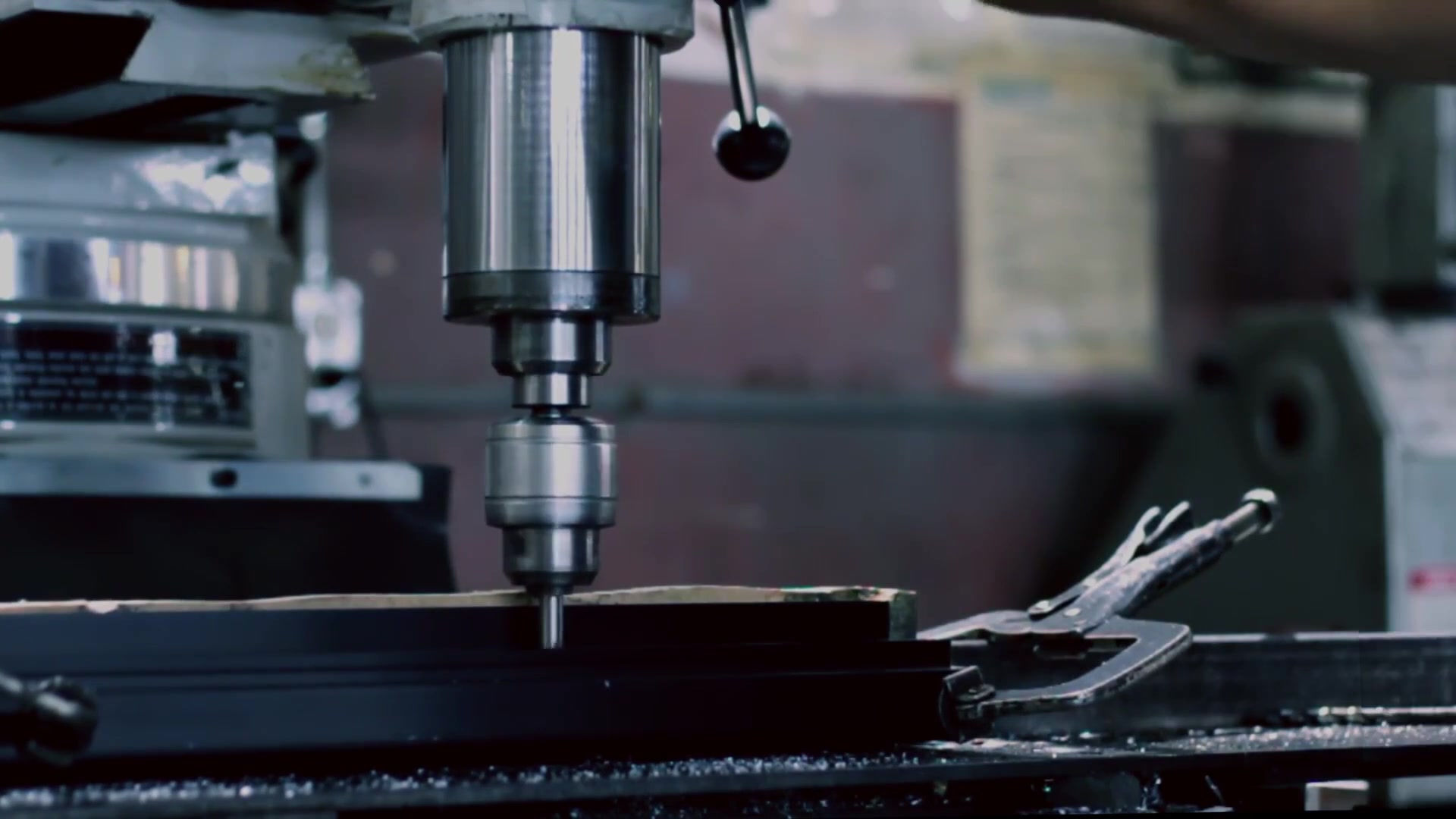
We supply custom manufactured and off-shelf jigs, fixtures and workholding tools for industrial applications, manufacturing lines, production lines, test and inspection lines, machine shops, R&D labs.......etc. Сложувалки, тела, алатки, решенија за работа, Производство на компоненти за мувла We offer custom manufactured and off-shelf jigs, fixtures and toolings for your workshop, factory, plant lab or other facility. The types of jigs you can purchase from us are: - Template Jig - Plate Jig - Angle-Plate Jig - Channel Jig - Diameter Jig - Leaf Jig - Ring Jig - Box Jig The types of fixtures we can supply you are: - Turning Fixtures - Milling Fixtures - Broaching Fixtures - Grinding Fixtures - Boring Fixtures - Tapping Fixtures - Duplex Fixtures - Welding Fixtures - Assembly Fixtures - Drilling Fixtures - Indexing Fixtures Some categories of industrial machine tools we manufacture and ship include: - Press tools and dies, shears - Extrusion dies - Molds, molding and casting tools - Forming tools - Shaping tools - Drilling, cutting, broaching, hobbing tools - Grinding tools - Machining, milling, turning tools - Holding and clamping tools CLICK ON BLUE TEXT BELOW TO DOWNLOAD CATALOGS & BROCHURES: EDM Tooling - Workholding Catalog Includes EDM Tooling System and Elements, EROWA Link, 3R-Link, UniClamp, Square Clamp, RefTool Holder, PIN Holder System, Clamping Elements, Swivel Block and Vises, CentroClamp, EDM Spare Parts....etc. Hose Crimping Machines and Tools We private label these with your brand name and logo if you wish. Crimp development team can assist you with the design and development of tooling for all of your crimping requirements. Hose Endforming Machines and Tools We private label these with your brand name and logo if you wish. Tool development team can assist you with the design and development of tooling for all of your end-forming tool requirements. Plastic Mold Components Catalog Here you will find off-shelf components, products that you can order and use in manufacturing your molds. These products are ideal for mold makers. Example products you can find here are ejector pins, slide units, pressure plugs, guide pins, sprue bushings, slide holding devices, wear plates, ejector sleeves.....etc. Private Label Auto Glass Repair and Replacement Systems We can private label these hand tools if you wish. In other words, we can put your company name, brand and label on them. This way you can promote your brand by reselling these to your customers. Private Label Hand Tools for Every Industry We can private label these hand tools if you wish. In other words, we can put your company name, brand and label on them. This way you can promote your brand by reselling these to your customers. Private Label Hand Tools - Hand Tool Cabinets We can private label these hand tools if you wish. In other words, we can put your company name, brand and label on them. This way you can promote your brand by reselling these to your customers. Private Label Power Tools for Every Industry We can private label these hand tools if you wish. In other words, we can put your company name, brand and label on them. This way you can promote your brand by reselling these to your customers. Wire EDM Tooling - Workholding Catalog Includes Wire EDM Clamping Systems & Sets, Corner Sets, Ruler & Spanner, EDM Clamping Block, 3D Swivel Head, Vise Set, WEDM Vises and Magnetic Tables, Multiclamp, Wire EDM Pendulum Holder, V-Block, ICS Adapter, Beams, Beam IF, Z-Flex, Turn and Index Table, Collet Chuck Holder, EDM Link and Adapter, 3 Jaw Scroll Chuck ....etc. Workholding Tools Catalog - 1 Check this catalog for our 100% EROWA and 3R compatible workholding tools. We accept OEM work, you can send us a drawing for evaluation. Workholding Tools Catalog - 2 Check this catalog for our Workholding Devices, Die and Mold Clamps, Clamping Elements, Clamping Kits, Fixture Clamps, Toggle Clamps, Milling & MC Vices, Pneumatic & Hydraulic Clamps, Milling & Grinding Accessories, Wire Cut EDM Workholders...etc. We accept OEM work, you can send us a drawing for evaluation. You may also find our following page link useful: Industrial Machines and Equipment Manufacturing КЛИКНЕТЕ Услуга за пронаоѓање на производи-локатор ПРЕТХОДНА СТРАНИЦА
- Display, Touchscreen, Monitors, LED, OLED, LCD, PDP, HMD, VFD, ELD
Display - Touchscreen - Monitors - LED - OLED - LCD - PDP - HMD - VFD - ELD - SED - Flat Panel Displays - AGS-TECH Inc. Производство и монтажа на екран и екран на допир и монитор We offer: • Custom displays including LED, OLED, LCD, PDP, VFD, ELD, SED, HMD, Laser TV, flat panel display of required dimensions and electro-optic specifications. Please click on highlighted text to download relevant brochures for our display, touchscreen, and monitor products. - Catalog for Vandal-Proof IP65/IP67/IP68 Keyboards, Keypads, Pointing Devices, ATM Pinpads, Medical & Military Keyboards and other similar Rugged Computer Peripherals - Kiosk Systems (We private label these with your brand name and logo if you wish) - Kiosk Systems Accessories Guide (We private label these with your brand name and logo if you wish) - LED display panels - LCD modules - Mobile Computers for Enterprises (We private label these with your brand name and logo if you wish) - Process Automation Solutions (This brochure includes some industrial display products. We private label these with your brand name and logo if you wish) Download our brochure for TRu Multi-Touch Monitors. This monitor product line consists of a range of desktop, open frame, slim line and large format multi-touch displays - from 15” to 70''. Built for quality, responsiveness, visual appeal, and durability, TRu Multi-Touch Monitors complement any multi-touch interactive solution. Click here for pricing If you would like to have LCD modules specially designed & manufactured according to your requirements, please fill out and email us: Custom design form for LCD modules If you would like to have LCD panels specially designed & manufactured according to your requirements, please fill out and email us: Custom design form for LCD panels • Custom touchscreen ( such as iPod ) • Among the custom products our engineers have developed are: - A contrast measuring station for liquid crystal displays. - A computerized centering station for television projection lenses Panels / Displays are electronic screens used to view data and / or graphics and are available in a variety of sizes and technologies. Here are the meanings of abbreviated terms related to display, touchscreen and monitor devices: LED: Light Emitting Diode LCD: Liquid Crystal Display PDP: Plasma Display Panel VFD: Vacuum Fluorescent Display OLED: Organic Light Emitting Diode ELD: Electroluminescent Display SED: Surface-conduction Electron-emitter Display HMD: Head Mounted Display A significant benefit of OLED display over liquid crystal display (LCD) is that OLED does not require a backlight to function. Therefore OLED display draws far less power and, when powered from a battery, can operate longer as compared to LCD. Because there is no need for a backlight, an OLED display can be much thinner than an LCD panel. However, degradation of OLED materials has limited their use as display, touchscreen and monitor. ELD works by exciting atoms by passing an electric current through them, and causing ELD to emit photons. By varying the material being excited, the colour of the emitted light can be changed. ELD is constructed using flat, opaque electrode strips running parallel to each other, covered by a layer of electroluminescent material, followed by another layer of electrodes, running perpendicular to the bottom layer. The top layer must be transparent in order to let light go through and escape. At each intersection, the material lights, thereby creating a pixel. ELDs are sometimes used as backlights in LCDs. They are also useful for creating soft ambient light, and for low-colour, high-contrast screens. A surface-conduction electron-emitter display (SED) is a flat panel display technology that uses surface conduction electron emitters for each individual display pixel. The surface conduction emitter emits electrons that excite a phosphor coating on the display panel, similar to cathode ray tube (CRT) televisions. In other words, SEDs use tiny cathode ray tubes behind every single pixel instead of one tube for the whole display, and can combine the slim form factor of LCDs and plasma displays with the superior viewing angles, contrast, black levels, color definition and pixel response time of CRTs. It is also widely claimed that SEDs consume less power than LCD displays. A head-mounted display or Helmet mounted display, both abbreviated 'HMD', is a display device, worn on the head or as part of a helmet, that has a small display optic in front of one or each eye. A typical HMD has either one or two small displays with lenses and semi-transparent mirrors embedded in a helmet, eye-glasses or visor. The display units are small and may include CRT, LCDs, Liquid Crystal on Silicon, or OLED. Sometimes multiple micro-displays are deployed to increase total resolution and field of view. HMDs differ in whether they can display just a computer generated image (CGI), show live images from the real world or a combination of both. Most HMDs display only a computer-generated image, sometimes referred to as a virtual image. Some HMDs allow superimposing a CGI upon a real-world view. This is sometimes referred to as augmented reality or mixed reality. Combining real-world view with CGI can be done by projecting the CGI through a partially reflective mirror and viewing the real world directly. For partially reflective mirrors, check our page on Passive Optical Components. This method is often called Optical See-Through. Combining real-world view with CGI can also be done electronically by accepting video from a camera and mixing it electronically with CGI. This method is often called Video See-Through. Major HMD applications include military, governmental (fire, police, etc.) and civilian/commercial (medicine, video gaming, sports, etc.). Military, police and firefighters use HMDs to display tactical information such as maps or thermal imaging data while viewing the real scene. HMDs are integrated into the cockpits of modern helicopters and fighter aircraft. They are fully integrated with the pilot's flying helmet and may include protective visors, night vision devices and displays of other symbols and information. Engineers and scientists use HMDs to provide stereoscopic views of CAD (Computer Aided Design) schematics. These systems are also used in the maintenance of complex systems, as they can give a technician an effectively ''x-ray vision'' by combining computer graphics such as system diagrams and imagery with the technician's natural vision. There are also applications in surgery, wherein a combination of radiographic data (CAT scans and MRI imaging) is combined with the surgeon's natural view of the operation. Examples of lower cost HMD devices can be seen with 3D games and entertainment applications. Such systems allow 'virtual' opponents to peek from real windows as a player moves about. Other interesting developments in display, touchscreen and monitor technologies AGS-TECH is interested are: Laser TV: Laser illumination technology remained too costly to be used in commercially viable consumer products and too poor in performance to replace lamps except in some rare ultra-high-end projectors. More recently however, companies demonstrated their laser illumination source for projection displays and a prototype rear-projection ''laser TV''. The first commercial Laser TV and subsequently others have been unveiled. First audiences who were shown reference clips from popular movies reported that they were blown away by a Laser TV's hitherto unseen color-display prowess. Some people even describe it as being too intense to the point of seeming artificial. Some other future display technologies will likely include carbon nanotubes and nanocrystal displays using quantum dots to make vibrant and flexible screens. As always, if you provide us details of your requirement and application, we can design and custom manufacture displays, touchscreens and monitors for you. Click here to download brochure of our Panel Meters - OICASCHINT Dowload brochure for our DESIGN PARTNERSHIP PROGRAM More information on our engineering work can be found on: http://www.ags-engineering.com КЛИКНЕТЕ Услуга за пронаоѓање на производи-локатор ПРЕТХОДНА СТРАНИЦА
- Surface Treatment and Modification - Surface Engineering - Hardening
Surface Treatment and Modification - Surface Engineering - Hardening - Plasma - Laser - Ion Implantation - Electron Beam Processing at AGS-TECH Површински третмани и модификација Surfaces cover everything. The appeal and functions material surfaces provide us are of utmost importance. Therefore SURFACE TREATMENT and SURFACE MODIFICATION are among our everyday industrial operations. Surface treatment & modification leads to enhanced surface properties and can be performed either as a final finishing operation or prior to a coating or joining operation. The processes of surface treatments and modification (also referred to as SURFACE ENGINEERING), tailor the surfaces of materials and products to: - Control friction and wear - Improve corrosion resistance - Enhance adhesion of subsequent coatings or joined parts - Change physical properties conductivity, resistivity, surface energy and reflection - Change chemical properties of surfaces by introducing functional groups - Change dimensions - Change the appearance, e.g., color, roughness…etc. - Clean and / or disinfect the surfaces Using surface treatment and modification, the functions and service lives of materials can be improved. Our common surface treatment and modification methods can be divided into two major categories: Surface Treatment and Modification That Covers Surfaces: Organic Coatings: The organic coatings apply paints, cements, laminates, fused powders and lubricants on the surfaces of materials. Inorganic Coatings: Our popular inorganic coatings are electroplating, autocatalytic plating (electroless platings), conversion coatings, thermal sprays, hot dipping, hardfacing, furnace fusing, thin film coatings such as SiO2, SiN on metal, glass, ceramics,….etc. Surface treatment and modification involving coatings is explained in detail under the related submenu, please click here Functional Coatings / Decorative Coatings / Thin Film / Thick Film Surface Treatment and Modification That Alters Surfaces: Here on this page we will concentrate on these. Not all of the surface treatment and modification techniques we describe below are on the micro or nano-scale, but we will nevertheless mention about them briefly since the basic objectives and methods are similar to significant extent to those that are on the micromanufacturing scale. Hardening: Selective surface hardening by laser, flame, induction and electron beam. High Energy Treatments: Some of our high energy treatments include ion implantation, laser glazing & fusion, and electron beam treatment. Thin Diffusion Treatments: Thin diffusion processes include ferritic-nitrocarburizing, boronizing, other high temperature reaction processes such as TiC, VC. Heavy Diffusion Treatments: Our heavy diffusion processes include carburizing, nitriding, and carbonitriding. Special Surface Treatments: Special treatments such as cryogenic, magnetic, and sonic treatments affect both the surfaces and the bulk materials. The selective hardening processes can be carried out by flame, induction, electron beam, laser beam. Large substrates are deep hardened using flame hardening. Induction hardening on the other hand is used for small parts. Laser and electron beam hardening are sometimes not distinguished from those in hardfacings or high-energy treatments. These surface treatment and modification processes are applicable only to steels that have sufficient carbon and alloy content to allow quench hardening. Cast irons, carbon steels, tool steels, and alloy steels are suitable for this surface treatment and modification method. Dimensions of parts are not significantly altered by these hardening surface treatments. Depth of hardening can vary from 250 microns to the whole section depth. However, in the whole section case, the section must be thin, less than 25 mm (1 in), or small, since the hardening processes require a rapid cooling of materials, sometimes within a second. This is difficult to achieve in large workpieces, and therefore in large sections, only the surfaces can be hardened. As a popular surface treatment and modification process we harden springs, knife blades, and surgical blades among many other products. High-energy processes are relatively new surface treatment and modification methods. Properties of surfaces are changed without changing the dimensions. Our popular high-energy surface treatment processes are electron beam treatment, ion implantation, and laser beam treatment. Electron Beam Treatment: Electron beam surface treatment alters the surface properties by rapid heating and rapid cooling — in the order of 10Exp6 Centigrade/sec (10exp6 Fahrenheit/sec) in a very shallow region around 100 microns near the material surface. Electron beam treatment can also be used in hardfacing to produce surface alloys. Ion Implantation: This surface treatment and modification method uses electron beam or plasma to convert gas atoms to ions with sufficient energy, and implant/insert the ions into atomic lattice of the substrate, accelerated by magnetic coils in a vacuum chamber. Vacuum makes it easier for ions to move freely in the chamber. The mismatch between implanted ions and the surface of the metal creates atomic defects that hardens the surface. Laser Beam Treatment: Like the electron beam surface treatment and modification, laser beam treatment alters the surface properties by rapid heating and rapid cooling in a very shallow region near the surface. This surface treatment & modification method can also be used in hardfacing to produce surface alloys. A know-how in Implant dosages and treatment parameters makes it possible for us to use these high energy surface treatment techniques in our fabrication plants. Thin Diffusion Surface Treatments: Ferritic nitrocarburizing is a case hardening process that diffuses nitrogen and carbon into ferrous metals at sub-critical temperatures. The processing temperature is usually at 565 Centigrade (1049 Fahrenheit). At this temperature steels and other ferrous alloys are still in a ferritic phase, which is advantageous compared to other case hardening processes that occur in the austenitic phase. The process is used to improve: •scuffing resistance •fatigue properties •corrosion resistance Very little shape distortion occurs during the hardening process thanks to the low processing temperatures. Boronizing, is the process where boron is introduced to a metal or alloy. It is a surface hardening and modification process by which boron atoms are diffused into the surface of a metal component. As a result the surface contains metal borides, such as iron borides and nickel borides. In their pure state these borides have extremely high hardness and wear resistance. Boronized metal parts are extremely wear resistant and will often last up to five times longer than components treated with conventional heat treatments such as hardening, carburizing, nitriding, nitrocarburizing or induction hardening. Heavy Diffusion Surface Treatment and Modification: If the carbon content is low (less than 0.25% for example) then we can increase the carbon content of the surface for hardening. The part can be either heat-treated by quenching in a liquid or cooled in still air depending on the properties desired. This method will only allow local hardening on the surface, but not in the core. This is sometimes very desirable because it allows for a hard surface with good wear properties as in gears, but has a tough inner core that will perform well under impact loading. In one of the surface treatment and modification techniques, namely Carburizing we add carbon to the surface. We expose the part to a Carbon rich atmosphere at an elevated temperature and allow diffusion to transfer the Carbon atoms into the steel. Diffusion will happen only if the steel has low carbon content, because diffusion works on the differential of the concentrations principle. Pack Carburizing: Parts are packed in a high carbon medium such as carbon powder and heated in a furnace for 12 to 72 hours at 900 Centigrade (1652 Fahrenheit). At these temperatures CO gas is produced which is a strong reducing agent. The reduction reaction occurs on the surface of the steel releasing carbon. The carbon is then diffused into the surface thanks to the high temperature. The Carbon on the surface is 0.7% to 1.2% depending on process conditions. The hardness achieved is 60 - 65 RC. The depth of the carburized case ranges from about 0.1 mm up to 1.5 mm. Pack carburizing requires good control of temperature uniformity and consistency in heating. Gas Carburizing: In this variant of surface treatment, Carbon Monoxide (CO) gas is supplied to a heated furnace and the reduction reaction of deposition of carbon takes place on the surface of the parts. This process overcomes most of the problems of pack carburizing. One concern however is the safe containment of the CO gas. Liquid Carburizing: The steel parts are immersed in a molten carbon rich bath. Nitriding is a surface treatment and modification process involving diffusion of Nitrogen into the surface of steel. Nitrogen forms Nitrides with elements such as Aluminum, Chromium, and Molybdenum. The parts are heat-treated and tempered before nitriding. The parts are then cleaned and heated in a furnace in an atmosphere of dissociated Ammonia (containing N and H) for 10 to 40 hours at 500-625 Centigrade (932 - 1157 Fahrenheit). Nitrogen diffuses into the steel and forms nitride alloys. This penetrates to a depth of up to 0.65 mm. The case is very hard and distortion is low. Since the case is thin, surface grinding is not recommended and therefore nitriding surface treatment may not be an option for surfaces with very smooth finishing requirements. Carbonitriding surface treatment and modification process is most suitable for low carbon alloy steels. In the carbonitriding process, both Carbon and Nitrogen are diffused into the surface. The parts are heated in an atmosphere of a hydrocarbon (such as methane or propane) mixed with Ammonia (NH3). Simply put, the process is a mix of Carburizing and Nitriding. Carbonitriding surface treatment is performed at temperatures of 760 - 870 Centigrade (1400 - 1598 Fahrenheit), It is then quenched in a natural gas (Oxygen free) atmosphere. The carbonitriding process is not suitable for high precision parts due to the distortions that are inherent. The hardness achieved is similar to carburizing (60 - 65 RC) but not as high as Nitriding (70 RC). The case depth is between 0.1 and 0.75 mm. The case is rich in Nitrides as well as Martensite. Subsequent tempering is needed to reduce brittleness. Special surface treatment and modification processes are in the early stages of development and their effectiveness is as yet unproven. They are: Cryogenic Treatment: Generally applied on hardened steels, slowly cool down the substrate to about -166 Centigrade (-300 Fahrenheit) to increase the density of the material and thus increase the wear resistance and dimension stability. Vibration Treatment: These intend to relieve thermal stress built-up in heat treatments through vibrations and increase the wear life. Magnetic Treatment: These intend to alter the line-up of atoms in materials through magnetic fields and hopefully improve the wear life. The effectiveness of these special surface treatment and modification techniques still remains to be proven. Also these three techniques above affect the bulk material besides surfaces. Please download our catalogs and brochures by clicking on the blue colored text below: - Private Label Nano Surface Protection Car Care Products We can label these products with your name and logo if you wish - Private Label Nano Surface Protection Industrial Products We can label these products with your name and logo if you wish - Private Label Nano Surface Protection Marine Products We can label these products with your name and logo if you wish - Private Label Nano Surface Protection Products We can label these products with your name and logo if you wish КЛИКНЕТЕ Услуга за пронаоѓање на производи-локатор ПРЕТХОДНА СТРАНИЦА
- News and Announcements - Employment Opportunities - New Product Launch
AGS-TECH Inc. News and Announcements - Employment Opportunities - New Product Launch - Corporate News - News about Advancements in Manufacturing and Technology Вести и соопштенија од AGS-TECH Inc November 5 - 2021: AGS-TECH, Inc. has become a value added reseller of QualityLine production Technologies, Ltd., a high-tech company that has developed an Artificial Intelligence based software solution that automatically integrates with your worldwide manufacturing data and creates an advanced diagnostics analytics for you. This tool is really different than any others in the market, because it can be implemented very quickly and easily, and will work with any type of equipment and data, data in any format coming from your sensors, saved manufacturing data sources, test stations, manual entry .....etc. No need to change any of your existing equipment to implement this software tool. Besides real time monitoring of key performance parameters, this AI software provides you root cause analytics, provides early warnings and alerts. There is no solution like this in the market. This tool has saved manufacturers plenty of cash reducing rejects, returns, reworks, downtime and gaining customers goodwill. Easy and quick ! To schedule a Discovery Call with us and to find out more about this powerful artıficial intelligence based manufacturing analytics tool: - Please fill out the downloadable QL Questionnaire from the blue link on the left and return to us by email to sales@agstech.net . - Have a look at the blue colored downloadable brochure links to get an idea about this powerful tool. QualityLine One Page Summary and QualityLine Summary Brochure - Also here is a short video that gets to the point: VIDEO of QUALITYLINE MANUFACTURING AN ALYTICS TOOL September 18 - 2021: AGS-TECH, Inc. has become an ATOP Industrial-Networking and Computing Distribution Partner. You can now order ATOP industrial networking and switching products from us. We offer your enterprise both off-the-shelf as well as custom tailored solutions. Please check our webpages and download respective brochures to help you select the best solution. Download our ATOP TECHNOLOGIES compact product brochure (Download ATOP Technologies Product List 2021) February 4 - 2020: Due to the coronavirus outbreak, we would like to inform our customers that some of our production taking place in China will resume on the 10th of February due to government precautions and measures to stop the spreading. We are sorry for the delay caused by this unfortunate event. July 19 -2018: AGS-TECH, Inc. has launched its renewed global procurement website. Potential suppliers of products and services please visit our procurement & purchasing site http://www.agsoutsourcing.com We encourage you to fill out the online supplier application form by clicking here: https://www.agsoutsourcing.com/online-supplier-application-platfor Filling out this form will enable us to evaluate you as a potential supplier. This is the most preferred way of becoming a supplier of AGS-TECH, Inc., its branches and affiliates. Whether you are a custom manufacturer of parts ad components, an engineering integrator, engineering consultant or services provider, or anything else you may think would be beneficial to us, this is the form you should fill out. January 31 - 2018: AGS-TECH Inc. launched its new website. We hope our existing customers and new potential customers will enjoy our new website and frequently visit us online. January 23 - 2017: Our new Free Space Optical Components brochure is now available for download under Optical / Fiber Optic Products menu or directly from the following link - FREE SPACE OPTICAL COMPONENTS BROCHURE We hope you will find it easy to scroll through our new product brochure. April 27 - 2015: AGS-TECH Inc. has currently the following open positions available. More information about these openings can be obtained from Dr. Zach Miller. Interested applicants, please email your interest along with resumes to info@agstech.net (put as title Career Opportunities) - Project Coordinator (At least a B.S. in Engineering, Physics or Materials Science required. Ideal candidate must have in-depth knowledge and hands-on experience in CNC machining, aluminum die casting, metal forging, joining and assembly processes such as welding, soldering, brazing, fastening, quality control, test and measurement techniques used in metallurgy. At least 5 years industrial experience in US or Canada and fluency in English, Chinese, Mandarin is required. Must have US or Canadian citizenship. - Project Coordinator (At least a B.S. in Engineering, Physics or Materials Science required. Ideal candidate must have in-depth knowledge and experience on fiber optic passive components, DWDM, beamsplitters, optical fiber amplifiers, fiber optic components assembly, quality control, test and measurement techniques such as power monitoring, OTDR, splicing tools, spectrum analyzers used in fiber optics. At least 5 years industrial experience in US or Canada and fluency in English, Chinese, Mandarin is required. Must have US or Canadian citizenship. April 24 - 2015: AGS-TECH Inc. website is currently being updated. Please be patient in case some pages cannot be accessed or have problems. We apologize for the temporary inconvenience this may cause during your visit. March 2014: AGS-TECH Inc. has currently the following open positions available. More information about these openings can be obtained from Dr. Zach Miller. Interested applicants, please email your interest along with resumes to info@agstech.net (put as title Career Opportunities) - Project Coordinator (At least a B.S. in Engineering, Physics or Materials Science required. Ideal candidate must know about machining, casting, precision assembly, quality control, test and measurement techniques used in metallurgy. Fluency in English, Chinese, Mandarin and / or Vietnamese is required) - Project Coordinator (At least a B.S. in Engineering, Physics or Materials Science required. Ideal candidate must know about machining, casting, precision assembly, quality control, test and measurement techniques used in metallurgy. Must speak German and English fluently. Candidates stationed and living in Germany are preferred) - Senior Systems Engineer (At least a B.S. in Engineering, Physics or Materials Science required, at least 5 years industrial experience in fiber optic communication systems preferred, fluency in English, Chinese, Mandarin required) • November 2013: AGS-TECH Inc. is hiring. Interested applicants, please email your interest along with resumes to info@agstech.net Open positions exist for: - Senior Design Engineer (Wireless Communication Systems) - Senior Systems Engineer (Wireless Communication Systems) - Materials or Chemical Engineer (Nanofabrication) - Project Coordinator (must speak Chinese and English fluently) - Project Coordinator (must speak German and English fluently. Candidates stationed and living in Germany are preferred) ПРЕТХОДНА СТРАНИЦА
- Sheet Metal Forming Fabrication, Stamping, Punching, Deep Drawing, CNC
Sheet Metal Forming and Fabrication, Stamping, Punching, Bending, Progressive Die, Spot Welding, Deep Drawing, Metal Blanking and Slitting at AGS-TECH Inc. Печатење и изработка на лим We offer sheet metal stamping, shaping, forming, bending, punching, blanking, slitting, perforating, notching, nibbling, shaving, pressworking, fabrication, deep drawing using single punch / single stroke dies as well as progressive dies and spinning, rubber forming and hydroforming; sheet metal cutting using water jet, plasma, laser, saw, flame; sheet metal assembly using welding, spot welding; sheet metal tube bulging and bending; sheet metal surface finishing including dip or spray painting, electrostatic powder coating, anodizing, plating, sputtering and more. Our services range from rapid sheet metal prototyping to high volume manufacturing. We recommend that you click here to DOWNLOAD our Schematic Illustrations of Sheet Metal Fabrication and Stamping Processes by AGS-TECH Inc. This will help you better understand the information we are providing you below. • SHEET METAL CUTTING : We offer CUTOFFS and PARTINGS. Cutoffs cut the sheet metal over one path at a time and there is basically no waste of material, whereas with partings the shape cannot be nestled precisely and therefore certain amount of material is wasted. One of our most popular processes is PUNCHING, where a piece of material round or other shape is cut out from sheet metal. The piece that is cut out is waste. Another version of punching is SLOTTING, where rectangular or elongated holes are punched. BLANKING on the other hand is the same process as punching, with the distinction of the piece being cut out is the work and is kept. FINE BLANKING, a superior version of blanking, creates cuts with close tolerances and straight smooth edges and does not require secondary operations for perfection of the workpiece. Another process we frequently use is SLITTING, which is a shearing process where sheet metal is cut by two opposing circular blades in a straight or curved path. Can opener is a simple example of the slitting process. Another popular process for us is PERFORATING, where many holes round or other shape are punched in sheet metal in a certain pattern. A typical example for a perforated product is metal filters with many holes for fluids. In NOTCHING, another sheet metal cutting process, we remove material from a work piece, starting at the edge or elsewhere and cut inward until the desired shape is obtained. It is a progressive process where each operation removes another piece until the desired contour is obtained. For small production runs we sometimes use a relatively slower process called NIBBLING which consists of many rapid punches of overlapping holes to make a larger more complex cut. In PROGRESSIVE CUTTING we use a series of different operations to obtain a single cut or a certain geometry. Finally SHAVING a secondary process helps us to improve edges of cuts that have already been made. It is used for cutting off the chips, rough edges on sheet metal work. • SHEET METAL BENDING : Besides cutting, bending is an essential process without which we would not be able to produce most products. Mostly a cold working operation but sometimes also performed when warm or hot. We use dies and press most of the time for this operation. In PROGRESSIVE BENDING we use a series of different punch and die operations to obtain a single bend or a certain geometry. AGS-TECH uses a variety of bending processes and makes the choice depending on the workpiece material, its size, thickness, desired size of bend, radius, curvature and angle of bend, location of bend, economy of operation, quantities to be manufactured…etc. We use V-BENDING where a V shaped punch forces the sheet metal into the V shaped die and bends it. Good for both very acute and obtuse angles and in between, including 90 degrees. Using wiping dies we perform EDGE BENDING. Our equipment enables us to obtain angles even larger than 90 degrees. In edge bending the workpiece is sandwiched between a pressure pad and the die, the area for bending is located on the die edge and the rest of the workpiece is held over space like a cantilever beam. When the punch acts on the cantilever portion, it is bent over the edge of the die. FLANGING is an edge bending process resulting in a 90 degree angle. Main goals of the operation are the elimination of sharp edges and obtaining geometric surfaces to ease the joining of parts. BEADING, another common edge bending process forms a curl over a part’s edge. HEMMING on the other hand results with an edge of the sheet that is bent completely over on itself. In SEAMING, the edges of two parts are bent over on each other and joined. DOUBLE SEAMING on the other hand provides watertight and airtight sheet metal joints. Similar to edge bending, a process called ROTARY BENDING deploys a cylinder with the desired angle cut out and serving as the punch. As the force is transmitted to the punch, it closes with the workpiece. The groove of the cylinder gives the cantilever portion the desired angle. The groove can have an angle smaller or larger than 90 degrees. In AIR BENDING, we do not need the lower die to have an angled groove. The sheet metal is supported by two surfaces on opposite sides and at a certain distance. The punch then applies a force at the right location and bends the workpiece. CHANNEL BENDING is performed using a channel shaped punch and die, and U-BEND is achieved with a U-shaped punch. OFFSET BENDING produces offsets on the sheet metal. ROLL BENDING, a technique good for thick work and bending of large pieces of metal plates, uses three rolls to feed and bend the plates to desired curvatures. Rolls are arranged so that the desired bend of the work is obtained. The distance and angle between the rolls is controlled to obtain the desired outcome. A moveable roll makes it possible to control the curvature. TUBE FORMING is another popular sheet metal bending operation involving multiple dies. Tubes are obtained after multiple actions. CORRUGATION is also performed by bending operations. Basically it is the symmetrical bending at regular intervals across an entire piece of sheet metal. Various shapes can be used for corrugating. Corrugated sheet metal is more rigid and has better resistance against bending and therefore has applications in the construction industry. SHEET METAL ROLL FORMING, a continuous manufacturing process is deployed to bend cross sections of a certain geometry using rolls and the work is bent in sequential steps, with the final roll completing the work. In some cases a single roll and in some cases a series of rolls are employed. • COMBINED SHEET METAL CUTTING & BENDING PROCESSES : These are the processes that cut and bend at the same time. In PIERCING, a hole is createdusing a pointed punch. As the punchwidens the hole in the sheet, the material is bent simultaneously into an internal flange for the hole. The flange obtained may have important functions. The LANCING operation on the other hand cuts and bends the sheet to create a raised geometry. • METAL TUBE BULGING AND BENDING : In BULGING some internal part of a hollow tube is pressurized, causing the tube to bulge outward. Since the tube is inside a die, the bulge geometry is controlled by the shape of the die. In STRETCH BENDING, a metal tube is stretched using forces parallel to the tube’s axis and bending forces to pull the tube over a form block. In DRAW BENDING, we clamp the tube near its end to a rotating form block that bends the tube while rotating. Lastly, in COMPRESSION BENDING the tube is held by force to a fixed form block, and a die bends it over the form block. • DEEP DRAWING : In one of our most popular operations, a punch, a matching die and a blank holder are used. The sheet metal blank is placed over the die opening and the punch moves towards the blank held by the blank holder. Once they come into contact, the punch forces the sheet metal into the die cavity to form the product. Deep drawing operation resembles cutting, however the clearance between the punch and die prevents the sheet from being cut. Another factor assuring the sheet is deep drawn and not cut are the rounded corners on the die and punch which prevents the shearing and cutting. To achieve a greater magnitude of deep drawing, a REDRAWING process is being deployed where a subsequent deep drawing takes place on a part that has already undergone a deep drawing process. In REVERSE REDRAWING, the deep drawn part is flipped over and drawn in the opposite direction. Deep drawing can provide irregular shaped objects such as domed, tapered or stepped cups, In EMBOSSING we use a male and female die pair to impress the sheet metal with a design or script. • SPINNING : An operation where a flat or preformed workpiece is held between a rotating mandrel and tail stock and a tool applies localized pressure to the work as it gradually moves up the mandrel. As a result, the workpiece is wrapped over the mandrel and takes its shape. We use this technique as an alternative to deep drawing where the quantity of an order is small, the parts are large (diameters up to 20 feet) and have unique curves. Even though the per piece prices are generally higher, the set-up costs for CNC spinning operation are low compared to deep drawing. To the contrary, deep drawing requires high initial investment for set-up, but the per piece costs are low when high quantity of parts are produced. Another version of this process is SHEAR SPINNING, where there is also metal flow within the workpiece. The metal flow will reduce the thickness of the workpiece as the process is carried out. Yet another related process is TUBE SPINNING, which is applied on cylindirical parts. Also in this process there is metal flow within the workpiece. The thickness is thus reduced and the tube’s length is increased. The tool can be moved to create features on the inside or outside of the tube. • RUBBER FORMING OF SHEET METAL : Rubber or polyurethane material is put in a container die and the work piece is placed on the surface of the rubber. A punch is then acted upon the work piece and forces it into the rubber. Since the pressure generated by the rubber is low, the depth of parts produced is limited. Since tooling costs are low, the process is suitable for low quantity production. • HYDROFORMING : Similar to rubber forming, in this process sheet metal work is pressed by a punch into a pressurized liquid inside a chamber. The sheet metal work is sandwiched between the punch and a rubber diaphragm. The diaphragm surrounds the workpiece completely and the pressure of the fluid forces it to form on the punch. Very deep draws even deeper than in the deep drawing process can be obtained with this technique. We manufacture single-punch dies as well as progessive dies depending on your part. Single stroke stamping dies are a cost effective method for producing large quantities of simple sheet metal parts such as washers quickly. Progressive dies or the deep drawing technique are used for manufacturing more complex geometries. Depending on your case, waterjet, laser or plasma cutting can be used to produce your sheet metal parts inexpensively, fast and accurately. Many suppliers have no idea about these alternative techniques or do not have it and therefore they go through lengthy and expensive ways of making dies and tools that only waste customers time and money. If you require custom built sheet metal components such as enclosures, electronic housings...etc as fast as within days, then contact us for our RAPID SHEET METAL PROTOTYPING service. КЛИКНЕТЕ Услуга за пронаоѓање на производи-локатор ПРЕТХОДНО МЕНИ
- Computer Integrated Manufacturing at AGS-TECH Inc, CAD & CAM, Lean Mfg
Computer Integrated Manufacturing (CIM) at AGS-TECH Inc. We offer Computer Aided Design (CAD), Computer Aided Manufacturing (CAM), Holonic Lean Manufacturing Компјутерски интегрирано производство во AGS-TECH Inc Our COMPUTER INTEGRATED MANUFACTURING (CIM) SYSTEMS interlink the functions of product design, research and development, production, assembly, inspection, quality control and others. AGS-TECH’s computer integrated manufacturing activities include: - COMPUTER-AIDED DESIGN (CAD) and ENGINEERING (CAE) - COMPUTER-AIDED MANUFACTURING (CAM) - COMPUTER-AIDED PROCESS PLANNING (CAPP) - COMPUTER SIMULATION of MANUFACTURING PROCESSES and SYSTEMS - GROUP TECHNOLOGY - CELLULAR MANUFACTURING - FLEXIBLE MANUFACTURING SYSTEMS (FMS) - HOLONIC MANUFACTURING - JUST-IN-TIME PRODUCTION (JIT) - LEAN MANUFACTURING - EFFICIENT COMMUNICATION NETWORKS - ARTIFICIAL INTELLIGENCE SYSTEMS COMPUTER-AIDED DESIGN (CAD) and ENGINEERING (CAE): We use computers to create design drawings and geometric models of products. Our powerful software like CATIA enables us to conduct engineering analysis to identify potential problems such as interference at mating surfaces during assembly. Other information such as materials, specifications, manufacturing instructions…etc. are also stored in the CAD database. Our customers can submit us their CAD drawings in any of the popular formats used in the industry, such as DFX, STL, IGES, STEP, PDES. Computer-Aided Engineering (CAE) on the other hand simplifies the creation of our database and allows various applications to share the information in the database. These shared applications include valuable information from finite-element analysis of stresses and deflections, temperature distribution in structures, NC data to name a few. After geometric modeling, the design is subjected to engineering analysis. This may consist of tasks such as analyzing stresses and strains, vibrations, deflections, heat transfer, distribution of temperature and dimensional tolerances. We use special software for these tasks. Prior to production, we may sometimes conduct experiments and measurements to verify the actual effects of loads, temperature and other factors on the component samples. Again, we do use special software packages with animation capabilities to identify potential problems with moving components in dynamic situations. This capability makes it possible to review and evaluate our designs in an effort to precisely dimension the parts and set appropriate production tolerances. Detail and working drawings are also produced with the help of these software tools we use. The database management systems which are built into our CAD systems allow our designers to identify, view and access parts from a library of stock parts. We must emphasize that CAD and CAE are two essential elements of our computer integrated manufacturing system. COMPUTER-AIDED MANUFACTURING (CAM): Without doubt, another essential element of our computer integrated manufacturing system is CAM which reduces cost and increases productivity. This involves all phases of manufacturing where we use computer technology and enhanced CATIA, including process and production planning, scheduling, manufacture, QC and management. Computer-aided design and computer-aided manufacturing are combined into CAD/CAM systems. This allows us to transfer information from the design stage to planning stage for the product manufacture without the need to manually reenter the data on part geometry. The database developed by CAD is further processed by CAM into the necessary data and instructions for operating and controlling production machinery, automated testing and inspection of products. CAD/CAM system allows us to display and visually check tool paths for possible tool collisions with fixtures and clamps in operations such as machining. Then, if needed, the tool path can be modified by the operator. Our CAD/CAM system is also capable of coding and classifying parts into groups that have similar shapes. COMPUTER-AIDED PROCESS PLANNING (CAPP): Process planning involves the selection of production methods, tooling, fixturing, machinery, operations sequence, standard processing times for individual operations and assembly methods. With our CAPP system we view the total operation as an integrated system with individual operations being coordinated with each other to produce the part. In our computer integrated manufacturing system, CAPP is an essential adjunct to CAD/CAM. It is vital for efficient planning and scheduling. The process-planning capabilities of computers can be integrated into the planning and control of production systems as a subsystem of computer-integrated manufacturing. These activities enable us capacity planning, control of inventory, purchasing and production scheduling. As part of our CAPP we have computer-based ERP system for effective planning and control of all the resources needed to take orders for products, produce them, ship them to the customers, service them, do the accounting and billing. Our ERP system is not only to the benefit of our corporation, but indirectly also to the benefit of our customers. COMPUTER SIMULATION of MANUFACTURING PROCESSES and SYSTEMS: We use finite-element analysis (FEA) for process simulations of specific manufacturing operations as well as for multiple processes and their interactions. Process viability is routinely studied using this tool. An example is assessing the formability and behavior of sheet metal in pressworking operation, process optimization by analyzing the metal-flow pattern in forging a blank and identifying potential defects. Yet another example application of FEA would be to improve mold design in casting operation to reduce and eliminate hot spots and minimize defects by achieving uniform cooling. Entire integrated manufacturing systems are also simulated to organize plant machinery, achieve better scheduling and routing. Optimizing the sequence of operations and organization of machinery helps us effectively reduce manufacturing costs in our computer integrated production environments. GROUP TECHNOLOGY: The group technology concept seeks to take advantage of the design and processing similarities among the parts to be produced. It is a valuable concept in our computer integrated lean manufacturing system. Many parts have similarities in their shape and method of manufacture. For example all shafts can be categorized into one family of parts. Similarly, all seals or flanges can be categorized into the same families of parts. Group technology helps us in economically manufacturing an ever-larger variety of products, each in smaller quantities as batch production. In other words, group technology is our key for inexpensive manufacturing of small quantity orders. In our cellular manufacturing, machines are arranged in an integrated efficient product flow line, named “group layout”. The manufacturing cell layout depends on the common features in parts. In our group technology system parts are identified and grouped into families by our computer controlled classification and coding system. This identification and grouping is done according to parts design and manufacturing attributes. Our advanced computer integrated decision-tree coding / hybrid coding combines both design and manufacturing attributes. Implementing group technology as part of our computer integrated manufacturing helps AGS-TECH Inc. by: -Making possible the standardization of part designs / minimization of design duplications. Our product designers can easily determine whether data on a similar part already exists in the computer database. New part designs can be developed using already existing similar designs, thereby saving on design costs. -Making data from our designers and planners stored in the computer integrated database available to less experienced personnel. -Enabling statistics on materials, processes, number of produced parts….etc. easy to be used to estimate manufacturing costs of similar parts and products. -Allowing efficient standardization and scheduling of process plans, grouping of orders for efficient production, better machine utilization, reducing setup times, facilitating the sharing of similar tools, fixtures and machines in the production of a family of parts, increasing overall quality in our computer integrated manufacturing facilities. -Improving productivity and reducing costs especially in small-batch production where it is needed the most. CELLULAR MANUFACTURING: Manufacturing cells are small units consisting of one or more computer integrated workstations. A workstation contains either one or several machines, each of which performs a different operation on the part. Manufacturing cells are effective in producing families of parts for which there is a relatively constant demand. Machine tools used in our manufacturing cells are generally lathes, milling machines, drills, grinders, machining centers, EDM, injection molding machines…etc. Automation is implemented in our computer integrated manufacturing cells, with automated loading/unloading of blanks and workpieces, automated changing of tools and dies, automated transfer of tools, dies and workpieces between workstations, automated scheduling and control of operations in the manufacturing cell. In addition, automated inspection and testing takes place in the cells. Computer integrated cellular manufacturing offers us reduced work in progress and economic savings, improved productivity, ability to detect quality issues right away without delay among other benefits. We also deploy computer integrated flexible manufacturing cells with CNC machines, machining centers and industrial robots. The flexibility of our manufacturing operations offers us the advantage of adapting to rapid changes in market demand and manufacturing more product variety in smaller quantities. We are able to process very different parts quickly in sequence. Our computer integrated cells can manufacture parts in batch sizes of 1 pc at a time with negligible delay between parts. These very short delays in between are for downloading new machining instructions. We have achieved building unattended computer integrated cells (unmanned) for economically manufacturing your small orders. FLEXIBLE MANUFACTURING SYSTEMS (FMS): Major elements of manufacturing are integrated into a highly automated system. Our FMS consist of a number of cells each containing an industrial robot that serves several CNC machines and an automated material-handling system, all interfaced with a central computer. Specific computer instructions for the manufacturing process can be downloaded for each successive part that passes through a workstation. Our computer integrated FMS systems can handle a variety of part configurations and produce them in any order. Furthermore the time required for changeover to a different part is very short and therefore we can respond very quickly to product and market-demand variations. Our computer controlled FMS systems carry out machining and assembly operations involving CNC machining, grinding, cutting, forming, powder metallurgy, forging, sheet metal forming, heat treatments, finishing, cleaning, part inspection. Material handling is controlled by central computer and carried out by automated guided vehicles, conveyors or other transfer mechanisms depending on production. Transportation of raw materials, blanks and parts in various stages of completion can be made to any machine, in any order at any time. Dynamic process planning and scheduling takes place, capable of responding to quick changes in product type. Our computer integrated dynamic scheduling system specifies the types of operations to be performed on each part and identifies the machines to be used. In our computer integrated FMS systems no setup time is wasted when switching between manufacturing operations. Different operations can be carried out in different orders and on different machines. HOLONIC MANUFACTURING: Components in our holonic manufacturing system are independent entities while being a subservient part of a hierarchical & computer integrated organization. In other words they are part of a “Whole”. Our manufacturing holons are autonomous and cooperative building blocks of a computer integrated manufacturing system for production, storage, and transfer of objects or information. Our computer integrated holarchies can be created and dissolved dynamically, depending on the current needs of the particular manufacturing operation. Our computer integrated manufacturing environment enables maximum flexibility through providing intelligence within holons to support all production and control functions required to complete production tasks and manage the equipment and systems. The computer integrated manufacturing system reconfigures into operational hierarchies to optimally produce products with holons being added or removed as needed. AGS-TECH factories consist of a number of resource holons available as separate entities in a resource pool. Examples are CNC milling machine and operator, CNC grinder and operator, CNC lathe and operator. When we receive a purchase order, an order holon is formed which starts to communicate and negotiate with our available resource holons. As an example, a work order may require the use of a CNC lathe, CNC grinder and an automated inspection station to organize them into a production holon. Production bottlenecks are identified and eliminated through computer integrated communication and negotiation between holons in the resource pool. JUST-IN-TIME PRODUCTION (JIT): As an option, we do provide Just-In-Time (JIT) production to our customers. Again, this is only an option we do offer to you in case you want or need it. Computer integrated JIT eliminates waste of materials, machines, capital, manpower and inventory throughout the manufacturing system. Our computer integrated JIT production involves: -Receiving supplies just in time to be used -Producing parts just in time to be turned into subassemblies -Producing subassemblies just in time to be assembled into finished products -Production and delivery of finished products just in time to be sold In our computer integrated JIT we produce parts to order while matching production with demand. There are no stockpiles, and no extra motions retrieving them from storage. In addition, parts are inspected in real time as they are being manufactured and are used within a short time period. This enables us to maintain control continuously and immediately to identify defective parts or process variations. Computer integrated JIT eliminates undesirable high inventory levels which can mask quality and production problems. All operations and resources that do not add value are eliminated. Our computer integrated JIT production offers our customers the option of eliminating the need to rent large warehouses and storage facilities. Computer integrated JIT results in high-quality parts and products at low cost. As part of our JIT system, we do use computer integrated KANBAN bar-coding system for production and conveyance of parts and components. On the other hand, JIT production may lead to higher production costs and higher per piece prices for our products. LEAN MANUFACTURING: This involves our systematic approach to identifying and eliminating waste and non-value added activities in every area of manufacturing through continuous improvement, and emphasizing product flow in a pull system rather than a push system. We continuously review all our activities from the viewpoint of our customers and optimize processes to maximize added value. Our computer integrated lean manufacturing activities include elimination or minimization of inventory, minimization of waiting times, maximization of our workers efficiency, elimination of unnecessary processes, minimization of product transportation and elimination of defects. EFFICIENT COMMUNICATION NETWORKS: For high level coordination and efficiency of operation in our computer integrated manufacturing we have an extensive, interactive high-speed communications network. We deploy LAN, WAN, WLAN and PANs for effective computer integrated communication between personnel, machines and buildings. Different networks are linked or integrated through gateways and bridges using secure file transfer protocols (FTP). ARTIFICIAL INTELLIGENCE SYSTEMS: This relatively new area of computer science finds applications to some degree in our computer integrated manufacturing systems. We take advantage of expert systems, computer machine vision and artificial neural networks. Expert systems are used in our computer-aided design, process planning and production scheduling. In our systems incorporating machine vision, computers and software are combined with cameras and optical sensors to perform operations like inspection, identification, sorting of parts and guiding robots. AGS-TECH, Inc. has become a value added reseller of QualityLine production Technologies, Ltd., a high-tech company that has developed an Artificial Intelligence based software solution that automatically integrates with your worldwide manufacturing data and creates an advanced diagnostics analytics for you. This tool is really different than any others in the market, because it can be implemented very quickly and easily, and will work with any type of equipment and data, data in any format coming from your sensors, saved manufacturing data sources, test stations, manual entry .....etc. No need to change any of your existing equipment to implement this software tool. Besides real time monitoring of key performance parameters, this AI software provides you root cause analytics, provides early warnings and alerts. There is no solution like this in the market. This tool has saved manufacturers plenty of cash reducing rejects, returns, reworks, downtime and gaining customers goodwill. Easy and quick ! To schedule a Discovery Call with us and to find out more about this powerful artıficial intelligence based manufacturing analytics tool: - Please fill out the downloadable QL Questionnaire from the blue link on the left and return to us by email to sales@agstech.net . - Have a look at the blue colored downloadable brochure links to get an idea about this powerful tool. QualityLine One Page Summary and QualityLine Summary Brochure - Also here is a short video that gets to the point: VIDEO of QUALITYLINE MANUFACTURING AN ALYTICS TOOL ПРЕТХОДНА СТРАНИЦА
- Manufacturing, Fabrication, Assembly, USA, AGS-TECH Inc.
AGS-TECH, Inc. Company Information - Manufacturing - Fabrication - Assembly - Moulding - Casting - CNC Machining - Extrusion - Forging - Electrical & Electronic AGS-TECH, Inc. е ваш Глобален прилагоден производител, интегратор, консолидатор, аутсорсинг партнер. Ние сме вашиот едношалтерски извор за производство, изработка, инженерство, консолидација, аутсорсинг. Информации за компанија - Manufacturing & Fabrication & Assembly at AGS-TECH Inc Добредојдовте во AGS-TECH Inc.! Ние сме воспоставен глобален лидер во снабдувањето со различни индустриски производи и услуги. Нашата разлика е во тоа што ние сме едношалтерски центар каде што можете да ги исполните поголемиот дел од вашите потреби за ПРОИЗВОДСТВО, ИЗРАБОТУВАЊЕ и СТАПУВАЊЕ, како што се КАЛАПИ, КАЛАТЕЊЕ НА ПЛАСТИКА И ГУМА, ИЗРАБОТУВАЊЕ НА матрици, ИЗРАБОТУВАЊЕ И ФОРМИРАЊЕ НА МЕТАЛ, ВРЕМЕЊЕ НА МЕТАЛ, ЛИЕЊЕ, МАШИНА, прав МЕТАЛУРГИЈА, МАШИНИ ЕЛЕМЕНТИ, ТЕХНИЧКО КЕРАМИЧКО производство, КОРИСТЕНА ЕЛЕКТРОНИКА, ОПТИКА, склопување со оптички влакна, ОПРЕМА ЗА ТЕСТИРАЊЕ и МЕТРОЛОГИЈА, ИНДУСТРИСКИ КОМПЈУТЕРИ, АВТОМАТИЧКА ОПРЕМА, и исто така, поддршка и деловни услуги. Не треба да купувате од многу места за да ги набавите сите делови и компоненти за вашите производи и проекти, не треба да се занимавате со секој добавувач посебно, да испраќате производи напред-назад... итн. Ова е премногу тешко и скапо. Имаме се за вас на едно место! Можеме да ги консолидираме сите за да ги намалиме трошоците за производство, изработка, склопување, пакување, етикетирање и испорака. Можеме да дизајнираме, произведуваме, склопуваме, квалификуваме, пакуваме, етикетираме, складираме и ги испраќаме до вас или до вашиот клиент. Ако немате шпедитер, можеме да се справиме со вашата испорака, увоз и царинска работа за вас. Ако сакате, можеме да го испратиме бродот со вашето име и лого. Бидејќи работиме на глобално ниво, можеме да ве снабдиме 1.) Подобар квалитет 2.) Подобри цени 3.) Подобри времиња на испорака. Нашата сила доаѓа од нашиот елитен тим составен од добро образовани, искусни и етаблирани лидери стационирани на нашите стратешки глобални локации. Нашата група за напредна технологија има мрежа со стотици глобално признати инженери и искусни технички менаџери во САД, ЕУ и Југоисточна Азија. Нашите напредни членови на техничкиот тим имаат повеќе патенти во нивните области на експертиза, многумина имаат десетици публикации во меѓународно признати списанија и се пронаоѓачи со дипломирани дипломи од врвни универзитети во светот. Постојано ги следиме најновите достигнувања во технологијата со цел да го задржиме нашето место како лидер. Имаме тимови во САД и ЕУ, како и во евтини земји како Кина, Индија, Тајван, Хонг Конг, Јужна Кореја каде што се произведуваат значителен дел од нашите производи. Нашиот маркетинг и Седиштето за продажба се наоѓа во САД. Додека нашиот Оддел за КК (контрола на квалитет) внимателно ги следи сите податоци за производство и испорака, анализирајќи ги трендовите во ефикасноста, приносот, враќањето, преработката и стапките на отпад во секоја фабрика и работи на континуирано подобрување, нашиот маркетинг тим постојано внимава на деловните и технолошките трендови. нови производи и можности за да можеме секогаш да им го понудиме најдоброто на нашите клиенти. Заштитата на интелектуалната сопственост на нашите клиенти е од најголема важност за нас и затоа пренесуваме информации само врз основа на „Треба да се знае“ во нашата организација. Нашите офшор канцеларии тесно соработуваат на дневна основа со нашиот главен тим во САД, така што сите сме подредени за истата цел: да ги направиме нашите клиенти да успеат и да станат поконкурентни на глобалниот пазар. Колку нашите клиенти стануваат поуспешни и поконкурентни, толку повеќе ќе успееме. Ако сте постоечки клиент, често прелистувајте ја нашата веб-локација за да најдете нови ажурирања за производи што ги објавуваме секогаш кога се достапни. Ако сте нови за нас, ве молиме посетете ја нашата веб-страница за подобро да ја разберете нашата компанија и испратете ни кој било од вашите технички цртежи, нацрти, листови со спецификации, примероци и од прва рака видете ги конкурентните цени што можеме да ги понудиме. Ги намаливме трошоците за набавка за над 50% или повеќе за повеќето наши клиенти. Зошто да плаќате повеќе во свет каде што можат да опстанат само најконкурентните компании? Бидете паметни и не дозволувајте другите да ве искинат и да ви наплаќаат апсурдни цени со бесмислено оправдување како што е обезбедување висококвалитетно производство и изработка можно само за високи цени, или со смешни тврдења како што е се Американец додека увезуваат 90% од нивните делови и само преетикетирајте ги... итн. Ваквите зборови за нас се глупости, бидејќи многу добро знаеме дека за мал дел од цената може да се понуди одличен квалитет и достава! Побарајте од нас референци за клиенти и со задоволство ќе ви ги обезбедиме. Во зависност од вашите потреби, ние можеме да ги произведуваме вашите производи или дома или на офшор. Знаеме многу добро кога домашното производство е поизводливо, а кога офшор е поизводливо. Ако сте најмногу заинтересирани за нашите инженерски и истражувачки и развојни способности наместо способностите за производство, изработка и склопување, тогаш ве покануваме да ја посетите нашата инженерска страница http://www.ags-engineering.com Прочитај повеќе Нашата производствена мисија од минатото и сегашноста Прочитај повеќе Вести и соопштенија од AGS-TECH, Inc. Прочитај повеќе Станете добавувач за инженерски интегратор и прилагоден производител AGS-TECH Inc. Прочитај повеќе AGS-TECH Разлика: најразновидните сопствени производители во светот, консолидатор, инженерски интегратор и партнер за надворешни извори Прочитај повеќе Автоматизација / Мала серија и масовно производство во AGS-TECH Inc Прочитај повеќе Компјутерски интегрирано производство во AGS-TECH Inc Прочитај повеќе Управување со квалитет во AGS-TECH Inc Прочитај повеќе Како цитираме проекти? Цитирање на сопствени произведени компоненти, склопови и производи Read More Логистика и испорака и складирање и испорака навреме во AGS-TECH Inc. Прочитај повеќе Општи услови за продажба во AGS-TECH Inc Прочитај повеќе Референци на клиентите Ние сме AGS-TECH Inc., ваш единствен извор за производство и изработка и инженерство и аутсорсинг и консолидација. Ние сме најразновидниот инженерски интегратор во светот кој ви нуди сопствено производство, подсклопување, склопување на производи и инженерски услуги.
- Seals, Fittings, Connections, Adaptors, Flanges, Pneumatics Hydraulics
Seals - Fittings - Connections - Adaptors - Flanges for Pneumatics Hydraulics and Vacuum - AGS-TECH Inc. Заптивки и фитинзи и стеги и врски и адаптери и прирабници и брзи спојки Vital components in pneumatic, hydraulic and vacuum systems are SEALS, FITTINGS, CONNECTIONS, ADAPTERS, QUICK COUPLINGS, CLAMPS, FLANGES. Depending on the application environment, standards requirements, and geometry of the application area there are a wide spectrum of these products readily available from our stock. On the other hand, for customers with special needs and requirements we are custom manufacturing seals, fittings, connections, adaptors, clamps and flanges for every possible pneumatics, hydraulics and vacuum application. If components within hydraulic systems never needed to be removed, we could simply braze or weld connections. However, it is inevitable that connections must be broken to allow servicing and replacing, so removable fittings and connections are a necessity for hydraulic, pneumatic and vacuum systems. Fittings seal fluids within hydraulic systems by one of two techniques: ALL-METAL FITTINGS rely on metal-to-metal contact, while O-RING TYPE FITTINGS rely on compressing an elastomeric seal. In both cases, tightening threads between mating halves of the fitting or between fitting and component forces two mating surfaces come together to form a high-pressure seal. ALL-METAL FITTINGS: Threads on pipe fittings are tapered and rely on the stress generated by forcing the tapered threads of the male half of the fittings into the female half of fittings. Pipe threads are prone to leakage because they are torque-sensitive. Over-tightening all-metal fittings distorts the threads too much and creates a path for leakage around the fittings threads. Pipe threads on all-metal fittings are also prone to loosening when exposed to vibration and wide temperature fluctuations. Pipe threads on fittings are tapered, and therefore repeated assembly and disassembly of the fittings aggravate the leakage problems by distorting the threads. Flare-type fittings are superior to pipe fittings and likely will remain the design of choice used in hydraulic systems. Tightening the nut draws the fittings into the flared end of the tubing, resulting in a positive seal between the flared tube face and the fitting body. The 37 degree flare fittings are designed for use with thin-wall to medium-thickness tubing in systems with operating pressures up to 3,000 psi and temperatures from -65 to 400 F. Because thick-wall tubing is difficult to form to produce the flare, it is not recommended for use with flare fittings. It is more compact than most other fittings and can easily be adapted to metric tubing. It is readily available and one of the most economical. The flareless fittings, gradually are gaining wider acceptance, because they require minimal tube preparation. Flareless fittings handle average fluid working pressures up to 3,000 psi and are more tolerant of vibration than other types of all-metal fittings. Tightening the fitting's nut onto the body draws a ferrule into the body. This compresses the ferrule around the tube, causing the ferrule to contact, then penetrate the outer circumference of the tube, creating a positive seal. Flareless fittings need to be used with medium or thick-walled tubing. O-RING TYPE FITTINGS: Fittings using O-rings for leak-tight connections continue to gain acceptance by equipment designers. Three basic types are available: SAE straight-thread O-ring boss fittings, face seal or flat-face O-ring (FFOR) fittings, and O-ring flange fittings. The choice between O-ring boss and FFOR fittings usually depends on such factors as fitting location, wrench clearance…etc. Flange connections generally are used with tubing that have an outer diameter greater than 7/8-inch or for applications involving extremely high pressures. O-ring boss fittings seat an O-ring between threads and wrench flats around the outer diameter (OD) of the male half of the connector. A leak-tight seal is formed against a machined seat on the female port. There are two groups of O-ring boss fittings: adjustable and non-adjustable fittings. Non-adjustable or non-orientable O-ring boss fittings include plugs and connectors. These are simply screwed into a port, and no alignment is needed. Adjustable fittings on the other hand, such as elbows and tees, need to be oriented in a specific direction. The basic design difference between the two types of O-ring boss fittings is that plugs and connectors have no locknuts and require no back-up washer to effectively seal a joint. They depend on their flanged annular area to push the O-ring into the port's tapered seal cavity and squeeze the O-ring for sealing the connection. On the other hand, adjustable fittings are screwed into the mating member, oriented in the required direction, and locked in place when a locknut is tightened. Tightening the locknut also forces a captive backup washer onto the O-ring, which forms the leak-tight seal. Assembly is always predictable, technicians need only make sure that the backup washer is firmly seated on the port's spot face surface when the assembly is completed and that it is tightened properly. The FFOR fittings form a seal between a flat and finished surface on the female half and an O-ring held in a recessed circular groove in the male half. Turning a captive threaded nut on the female half draws the two halves together while compressing the O-ring. Fittings with O-ring seals offer some advantages over metal-to-metal fittings. All-metal fittings are more susceptible to leakage because they must be tightened to within a higher, yet narrower torque range. This makes it easier to strip threads or crack or distort fitting components, which prevents proper sealing. The rubber-to-metal seal in O-ring fittings does not distort any metal parts and provides a feel on our fingers when the connection is tight. All-metal fittings tighten more gradually, so technicians may find it more difficult detecting when a connection is tight enough but not too tight. Disadvantages are that O-ring fittings are more expensive than all-metal fittings, and care must be exercised during installation to ensure that the O-ring doesn't fall out or get damaged when the assemblies are connected. In addition, O-rings are not interchangeable among all couplings. Selecting the wrong O-ring or reusing one that has been deformed or damaged can result in leakage in fittings. Once an O-ring has been used in a fitting, it is not reusable, even though it may appear free of distortions. FLANGES: We offer flanges individually or as a complete set for a number of applications in a range of sizes and types. Stock is kept of Flanges, Counter-flanges, 90 degree flanges, Split flanges, Threaded flanges. Fittings for tubing larger than 1-in. OD have to be tightened with large hexnuts which requires a large wrench to apply sufficient torque to tighten the fittings properly. To install such large fittings, the necessary space needs to be given to workers to swing large wrenches. Worker strength and fatigue could also affect proper assembly. Wrench extensions may be needed for some workers to exert an applicable amount of torque. Split-flange fittings are available so that they overcome these problems. Split-flange fittings use an O-ring to seal a joint and contain pressurized fluid. An elastomeric O-ring sits in a groove on a flange and mates with a flat surface on a port - an arrangement similar to the FFOR fitting. The O-ring flange is attached to the port using four mounting bolts that tighten down onto flange clamps. This eliminates the need for large wrenches when connecting large-diameter components. When installing flange connections, it is important to apply even torque on the four flange bolts to avoid creating a gap through which the O-ring can extrude under high pressure. A split-flange fitting consists generally of four elements: a flanged head connected permanently (generally welded or brazed) to the tube, an O-ring that fits into a groove machined into the end face of the flange, and two mating clamp halves with appropriate bolts to connect the split-flange assembly to a mating surface. The clamp halves do not actually contact the mating surfaces. A critical operation during assembly of a split-flange fitting to its mating surface is to make sure that the four fastening bolts are tightened gradually and evenly in a cross pattern. CLAMPS: A variety of clamping solutions for hose and tube are available, with either a profiled or smooth inner surface in a wide range of sizes. All necessary components can be supplied according to the specific application including, Clamp jaws, Bolts, Stacking bolts, Weld plates, Top plates, Rail. Our hydraulic and pneumatic clamps enable a more efficient installation, resulting in a clean pipe layout, with effective vibration and noise reduction. AGS-TECH hydraulic and pneumatic clamping products ensure repeatability of clamping and consistent clamping forces to avoid part movement and tool breakage. We stock a wide variety of clamping components (inch and metric-based), precision 7 MPa (70 bar) hydraulic clamping systems and professional-grade pneumatic work-holding devices. Our hydraulic clamping products are rated up to 5,000 psi operating pressure that can securely clamp parts in many applications ranging from automotive to welding, and from consumer to industrial markets. Our selection of pneumatic clamping systems provide air-operated holding for high-production environments and applications that require consistent clamping forces. Pneumatic clamps are used for holding and fixturing in assembly, machining, plastics manufacturing, automation and welding applications. We can help you determine work-holding solutions based on your part size, amount of clamp forces needed and other factors. As the World’s most diverse custom manufacturer, outsourcing partner and engineering integrator, we can design and manufacture custom pneumatic and hydraulic clamps for you. ADAPTERS: AGS-TECH offers adapters that provide leak free solutions. Adapters include hydraulic, pneumatic & instrumentation. Our adapters are manufactured to meet or exceed the industrial standards requirements of SAE, ISO, DIN, DOT and JIS. A wide range of adapter styles are available including: Swivel Adapters, Steel and Stainless Steel Pipe Adapters and Industrial Fittings, Brass Pipe Adapters, Brass and Plastic Industrial Fittings, High Purity and Process Adapters, Angled Flare Adapters. QUICK COUPLINGS: We offer quick connect / disconnect couplings for hydraulic, pneumatic and medical applications. Quick disconnect couplings are used to connect and disconnect hydraulic or pneumatic lines quickly and easily without using any tools. Various models are available: Non spill and double-shut-off quick couplings, Connect under pressure quick couplings, Thermoplastic quick couplings, Test port quick couplings, agricultural quick couplings,….and more. SEALS: Hydraulic and pneumatic seals are designed for the reciprocating motion which is common in hydraulic and pneumatic applications, such as cylinders. Hydraulic and pneumatic seals include Piston seals, Rod seals, U-cups, Vee, Cup, W, Piston, Flange packings. Hydraulic seals are designed for high-pressure dynamic applications such as hydraulic cylinders. Pneumatic seals are used in pneumatic cylinders and valves and are usually designed for lower operating pressures compared to hydraulic seals. Pneumatic applications demand however higher operating speeds and lower friction seals compared to hydraulic applications. Seals may be used for rotary and reciprocating motion. Some hydraulic seals and pneumatic seals are composite and are two-or multi-part manufactured as an integral unit. A typical composite seal consists of an integral PTFE ring and an elastomer ring, providing the properties of an elastomeric ring with a rigid, low friction (PTFE) working face. Our seals can have a variety of different cross sections. Common sealing orientation and directions for hydraulic and pneumatic seals include 1.) Rod Seals which are radial seals. The seal is press-fit into a housing bore with the sealing lip contacting the shaft. Also referred to as a shaft seal. 2.) Piston seals which are radial seals. The seal is fit onto a shaft with the sealing lip contacting the housing bore. V-rings are considered external lip seals, 3.) Symmetric seals are symmetrical and work equally well as a rod or piston seal, 4.) An axial seal seals axially against a housing or machine component. Sealing direction is relevant to hydraulic and pneumatic seals used in applications with axial motion, such as cylinders and pistons. The action can be single or double. Single acting, or unidirectional seals, offer an effective seal in one axial direction only, whereas double acting, or bi-directional seals, are effective when sealing in both directions. In order to seal in both directions for a reciprocating motion, more than one seal must be used. Features for hydraulic and pneumatic seals include spring loaded, integral wiper, and split seal. Some important dimensions to consider when you specify hydraulic and pneumatic seals are: • Shaft outer diameter or seal inner diameter • Housing bore diameter or seal outer diameter • Axial cross section or thickness • Radial cross section Important service limit parameters to consider when purchasing seals are: • Maximum operating speed • Maximum operating pressure • Vacuum rating • Operation temperature Popular material choices for rubber sealing elements for hydraulics and pneumatics include: • Ethylene Acrylic • EDPM Rubber • Fluoroelastomer and Fluorosilicone • Nitrile • Nylon or Polyamide • Polychloroprene • Polyoxymethylene • Polytetrafluoroethylene (PTFE) • Polyurethane / Urethane • Natural Rubber Some seal material choices are: • Sintered Bronze • Stainless Steel • Cast Iron • Felt • Leather Standards related to seals are: BS 6241 - Specifications for dimensions of housing for hydraulic seals incorporating bearing rings for reciprocating applications ISO 7632 - Road vehicles - elastomeric seals GOST 14896 - Rubber U-packing seals for hydraulic devices You can download relevant product brochures from the links below: Pneumatic Fittings Pneumatic Air Tubing Connectors Adapters Couplings Splitters and Accessories Private Label Pneumatic Compressed Air Hoses Fittings (We private label these with your brand name and logo if you wish) Private Label Pneumatic Quick Couplings, Plugs and Nipples (We private label these with your brand name and logo if you wish) Information on our facility producing ceramic to metal fittings, hermetic sealing, vacuum feedthroughs, high and ultrahigh vacuum and fluid control components can be found here: Fluid Control Factory Brochure КЛИКНЕТЕ Услуга за пронаоѓање на производи-локатор ПРЕТХОДНА СТРАНИЦА
- Gears and Gear Drives, Gear Assembly, Spur Gears, Rack & Pinion
Gears and Gear Drives, Gear Assembly, Spur Gears, Rack & Pinion & Bevel Gears, Miter, Worms, Machine Elements Manufacturing at AGS-TECH Inc. Склопување на запчаници и погон на менувачот AGS-TECH Inc. offers you power transmission components including GEARS & GEAR DRIVES. Gears transmit motion, rotating or reciprocating, from one machine part to another. Where necessary, gears reduce or increase the revolutions of the shafts. Basically gears are rolling cylindrical or conic-shaped components with teeth on their contact surfaces to ensure positive motion. Please note that gears are the most durable and rugged of all mechanical drives. Most heavy-duty machine drives and automobiles, transportation vehicles preferably use gears rather than belts or chains. We have many kinds of gears. - SPUR GEARS: These gears connect parallel shafts. Spur gear proportions and teeth shape are standardized. Gear drives need to be operated under a variety of conditions and therefore it is very difficult to determine the best gear set for a particular application. The easiest is to select from stocked standard gears with an adequate load rating. Approximate power ratings for spur gears of various sizes (number of teeth) at several operating speeds (revolutions/minute) are available in our catalogs. For gears with sizes and speeds not listed, ratings can be estimated from values shown on special tables and graphs. Service class and factor for spur gears is also a factor in the selection process. - RACK GEARS: These gears convert spur gears motion to reciprocating or linear motion. A rack gear is a straight bar with teeth that engage the teeth on a spur gear. The specifications for the teeth of the rack gear are given in the same manner as for spur gears, because rack gears can be imagined as spur gears having an infinite pitch diameter. Basically, all circular dimensions of spur gears become linear fir rack gears. - BEVEL GEARS (MITER GEARS and else): These gears connect shafts whose axes intersect. The axes of bevel gears may intersect at an angle, but the most common angle is 90 degrees. The teeth of bevel gears are the same shape as spur gear teeth, but taper toward the cone apex. Miter gears are bevel gears having the same diametral pitch or module, pressure angle and number of teeth. - WORMS and WORM GEARS: These gears connect shafts whose axes do not intersect. Worm gears are used to transmit power between two shafts that are at right angles to each other and are nonintersecting. Teeth on the worm gear are curved to conform with the teeth on the worm. The lead angle on worms should be between 25 and 45 degrees to be efficient in power transmission. Multi-thread worms with one to eight threads are used. - PINION GEARS: The smaller of the two gears is called pinion gear. Often a gear and pinion are made of different materials for better efficiency and durability. The pinion gear is made of a stronger material because the teeth on the pinion gear come into contact more times than the teeth on the other gear. We have standard catalog items as well the capability to manufacture gears according to your request and specifications. We also offer gear design, assembly and manufacturing. Gear design is very complicated because designers need to be dealing with problems such as strength, wear and material selection. The majority of our gears are made of cast iron, steel, brass, bronze or plastic. We have five levels of tutorial for gears, please read them in the given order. If you are not familiar with gears and gear drives, these tutorials below will help you in designing your product. If you prefer, we can also assist you in choosing the right gears for your design. Click on highlighted text below to download the relevant product catalog: - Introductory guide for gears - Basic guide for gears - Guide for practical use of gears - Introduction to gears - Technical reference guide for gears To help you compare applicable standards related to gears in different parts of the World, here you can download: Equivalency Tables for Standards of Raw Material and Gear Precision Grade Once more, we would like to repeat that in order to purchase gears from us, you do not need to have a particular part number, size of gear….etc handy. You do not need to be an expert in gears and gear drives. All you need is really to provide us as much information as possible regarding your application, dimensional limitations where the gears need to be installed, maybe photos of your system…and we will help you. We use computer software packages for the integrated design and manufacture of generalized gear pairs. These gear pairs include cylindrical, bevel, skew-axis, worm and worm wheel, along with non-circular gear pairs. The software we use is based on mathematical relations that differ from established standards and practice. This enables the following features: • any face width • any gear ratio (linear & nonlinear) • any number of teeth • any spiral angle • any shaft center distance • any shaft angle • any tooth profile. These mathematical relations seamlessly encompass different gear types to design and manufacture gear pairs. Here are some of our off-shelf gear and gear drive brochures and catalogs. Click on colored text to download: - Gears - Worm Gears - Worms and Gear Racks - Slewing Drives - Slewing Rings (some have internal or external gears) - Worm Gear Speed Reducers - WP Model - Worm Gear Speed Reducers - NMRV Model - T-Type Spiral Bevel Gear Redirector - Worm Gear Screw Jacks Reference Code: OICASKHK КЛИКНЕТЕ Услуга за пронаоѓање на производи-локатор ПРЕТХОДНА СТРАНИЦА
- Diamond Tools , USA , AGS-TECH Inc.
AGS-TECH Inc. manufactures and supplies diamond tools, including CNC vacuum brazed tools, CNC sintered tools, diamond contour blade, diamond ring saw blade, diamond segments, segmented saw blade, continuous rim blades, turbo saw blades, brazed saw blades, laser welded saw blade, cup grinding wheels, diamond core drill. Дијамантски алатки Please click on the blue highlighted text on diamond tools of interest below to download related brochure. CNC Vacuum Brazed Tools CNC Sintered Tools Diamond Contour Blade Diamond Ring Saw Blade Diamond Segments Segmented Saw Blade Continuous Rim Blades Turbo Saw Blades Brazed Saw Blades Laser Welded Saw Blade Diamond Tuck Point Blade Cup Grinding Wheels Diamond Saw Blade Kit Diamond Core Drill Bits Diamond Fickert Diamond Blade with Holder Diamond Polishing Tools Diamond Mound Point Diamond Files Electroplated Saw Blade Resin Grinding Wheels PRICE: Depends on model and quantity of order. For pricing on special designs of diamond tools, please either provide us your technical blueprints or let us know your application and let us design the custom diamond tool for you. Since we carry a wide variety of diamond tools with different dimensions, applications and material; it is impossible to list them here. We encourage you to email or call us so we can determine which product is the best fit for you. When contacting us, please make sure to inform us about some vital details: - Application - Material grade - Dimensions - Finish - Packaging requirements - Labeling requirements - Quantity needed per order / per year Private Label Power Tool Accessories This brochure includes some diamong tools. We can private label these hand tools if you wish. In other words, we can put your company name, brand and label on them. This way you can promote your brand by reselling these to your customers. КЛИКНЕТЕ ТУКА за да ги преземете нашите технички способности и референтниот водич за специјализирани алатки за сечење, дупчење, мелење, обликување, обликување, полирање што се користат во медицински, стоматолошки, прецизни инструменти, печат на метал, обликување матрица и други индустриски апликации. КЛИКНЕТЕ Услуга за пронаоѓање на производи-локатор Кликнете овде за да отидете во менито Алатки за сечење, дупчење, брусење, преклопување, полирање, коцки и обликување Уп. Шифра: OICASOSTAR
- Equipment to Cut Drill Polish , USA , AGS-TECH Inc.
AGS-TECH Inc. is a supplier of equipment to cut, drill and polish materials such as glass, semiconductors, wood, masonry...etc. Contact us for mini lathe, mini milling machine, ultrasonic drill, mini hobbing machine, desktop stamping press, desktop laser cutter, mini waterjet cutter, desktop plasma cutting machine... Опрема за сечење, дупчење, полирање Please click on the products of interest below to download related brochures. Equipment we supply to cut, drill and polish are generally tabletop, compact, small and economical, yet efficient, versatile, high return on investment type equipment suitable for prototype manufacturing, research & development and small scale industrial production. Our strength is also in customizing equipment to cut drill and polish. We are capable of building equipment for you which you may not be able to find readily in the market. - Hose-Cut-Off-Skive-Machine (We private label these with your brand name and logo if you wish) - Mini Lathe - Mini Milling Machine - Mini Hobbing Machine - Mini Stamping Press - Mini Laser Cutter - Mini Waterjet Cutter - Mini Plasma Cutter - Power Tools for Every Industry (We private label these with your brand name and logo if you wish) - Servo C-Frame Utility Press (We private label these with your brand name and logo if you wish) - Ultrasonic Drill Since we offer a wide variety of equipment for cutting, dicing, drilling, lapping, polishing, shaping; it is impossible to list them all here. From time to time we introduce also new equipment to the market. We encourage you to email or call us so we can jointly determine which product is the best fit for you. When you contact us, please make sure to inform us about: - Your application - Type and grade of material to be processed - Dimensions of material to be processed - Finish required after processing - Quantity / Number of units to be processed per hour or day. КЛИКНЕТЕ ТУКА за да ги преземете нашите технички способности и референтниот водич за специјализирани алатки за сечење, дупчење, мелење, обликување, обликување, полирање што се користат во медицински, стоматолошки, прецизни инструменти, печат на метал, обликување матрица и други индустриски апликации. КЛИКНЕТЕ Услуга за пронаоѓање на производи-локатор Кликнете овде за да отидете во менито Алатки за сечење, дупчење, брусење, преклопување, полирање, коцки и обликување Уп. Код: oicaszhengzhouhongtuo, oicaslzqtool
- Manufacturing Pneumatics Hydraulics, Pneumatic Hydraulic Products
Manufacturing Pneumatic Hydraulic Vacuum Products, Custom Pneumatics, Hydrolics, Control Valves, Pipes, Tubes, Hoses, Bellows, Seals & Fittings & Connections Пневматика и хидраулика и вакуумски производи Прочитај повеќе Компресори и пумпи и мотори Прочитај повеќе Вентили за пневматика и хидраулика и вакуум Прочитај повеќе Цевки и цевки и црева и мевови и компоненти за дистрибуција Прочитај повеќе Заптивки и фитинзи и стеги и врски и адаптери и прирабници и брзи спојки Прочитај повеќе Filters & Treatment Components Прочитај повеќе Активатори Акумулатори Прочитај повеќе Резервоари и комори за хидраулика и пневматика и вакуум Прочитај повеќе Сервисни и поправки комплети за пневматика и хидраулика и вакуум Прочитај повеќе Системски компоненти за пневматика и хидраулика и вакуум Прочитај повеќе Алатки за хидраулика и пневматика и вакуум AGS-TECH supplies off-shelf as well as custom manufactured PNEUMATICS & HYDRAULICS and VACUUM PRODUCTS. We offer original brand name components, generic brand and AGS-TECH brand pneumatic, hydraulic and vacuum products. Regardless of which category, our components are manufactured at plants certified to international standards and meet related industrial standards. Here is a brief summary of our pneumatic, hydraulic and vacuum products. You can find more detailed information by clicking on the submenu titles on the side. COMPRESSORS & PUMPS & MOTORS: A variety of these are offered off-shelf for pneumatic, hydraulic and vacuum applications. We have specialized compressors, pumps and motors for each type of application. You may choose the products you need in our downloadable brochures on relevant pages or if you are unsure, you may describe us your needs and applications and we can offer you the suitable pneumatics, hydraulics and vacuum products. For some of our compressors, pumps and motors we are capable to make modifications or manufacture them custom tailored to your applications. To give you a feeling of the wide spectrum of compressors, pumps and motors we can supply, here are a few types: Oilless air motors, cast iron and aluminum rotary vane air motors, piston air compressor / vacuum pump, positive displacement blowers, diaphragm compressor, hydraulic gear pump, hydraulic radial piston pump, hydraulic track drive motors. CONTROL VALVES: Models of these for either hydraulics, pneumatics or vacuum are available. Similar to our other products, you can order off-shelf as well as custom manufactured versions. The types we carry range from air cylinder speed control valves to filtered ball valves, from directional control valves to auxiliary valves and from angle valves to venting valves. PIPES & TUBES & HOSES & BELLOWS: These are manufactured according to the application environment and conditions. For example hydraulic tubes for A/C refrigeration requires the tube material to withstand cold temperatures, while a hydraulic beverage dispensing tube needs to be food grade and made from materials that do not pose health hazard. On the other hand, the shape of pneumatic/hydraulic/vacuum tubes and hoses shows also a variety, such as coiled air hose assemblies which are easy to handle because of their compactness and coiled structure and ability to extend when needed. Bellows used for vacuum systems need to have perfect sealing capability to maintain high vacuum while being flexible and be able to be bent when needed. SEALS & FITTINGS & CONNECTIONS & ADAPTORS & FLANGES: These may be overlooked because of being only a small component in the entire pneumatic / hydraulic or vacuum system. However even the smallest member of a system is very critical as a simple leak of air through a seal or fitting can easily prevent a quality vacuum to be achieved in a high vacuum system and result in costly repairs and production re-runs. On the other hand, a small leak of a toxic gas in a pneumatic gas delivery line can result in a disaster. Once again, our task is to understand our customers needs and requirements very well and provide them the exact pneumatics & hydraulics or vacuum product matching their application. FILTERS & TREATMENT COMPONENTS: Without filtering and treatment of the liquids and gases, a hydraulic, pneumatic or vacuum system cannot fulfill its tasks to full extent. As an example, a vacuum system will need air intake after an operation is complete so the system can be opened. If the air entering the vacuum system is dirty and contains oils, it will be very difficult to obtain high vacuum for the next operation cycle. A filter at air intake can eliminate such problems. On the other hand, breather filters are common in hydraulics. Filters must be of highest quality and suitable for their intended use. For example they need to be reliable and not pose risks of contaminating the pneumatic, hydraulic or vacuum system they are used in. Their inner content (such as dessicant dryers) and components cannot degrade quickly when exposed to certain chemicals, oils or humidity. On the other hand, some systems, such as it is the case in some pneumatic systems, do require lubrication of the air and therefore compressed air lubricators are used. Other examples of treatment components are electronic proportional regulators used in pneumatics, pneumatic coalescing filter elements, pneumatic oil/water separators. ACTUATORS & ACCUMULATORS: A hydraulic actuator is a cylinder or fluid motor that converts hydraulic power into useful mechanical work. The mechanical motion produced can be linear, rotary, or oscillatory. Operation exhibits high force capability, high power per unit weight and volume, good mechanical stiffness, and a high dynamic response. These properties lead to a wide use in precision control systems, heavy-duty machine tools, transportation, marine, and aerospace applications. Similarly a pneumatic actuator converts energy that is typically in the form of compressed air into mechanical motion. The motion can be rotary or linear, depending on the type of pneumatic actuator. Accumulators usually are installed in hydraulic systems to store energy and to smooth out pulsations. A hydraulic system with an accumulator can use a smaller pump because the accumulator stores energy from the pump during periods of low demand. This accumulated energy is available for instantaneous use, released upon demand at a much higher rate than could be supplied by the hydraulic pump alone. Accumulators can also be used as surge or pulsation absorbers. Accumulators can cushion hydraulic hammer, reducing shocks caused by rapid operation or sudden starting and stopping of power cylinders in a hydraulic circuit. A variety of models of these for either hydraulics, pneumatics are available. Similar to our other products, you can order off-shelf as well as custom manufactured actuator and accumulator versions. RESERVOIRS & CHAMBERS FOR HYDRAULICS & PNEUMATICS & VACUUM: Hydraulic systems need a finite amount of liquid fluid that must be stored and reused continually as the circuit works. Because of this, part of any hydraulic circuit is a storage reservoir or tank. This tank may be part of the machine framework or a separate stand-alone unit. Similarly, a pneumatic or air receiver tank is an integral and important part of any compressed air system. Typically a receiver tank is sized at 6-10 times the flow rate of the system. In a pneumatic compressed air system, a receiver tank can provide several benefits such as: -Acting as a reservoir of compressed air for peak demands. -A pneumatic receiver tank can help remove water from the system by giving the air a chance to cool. -A pneumatic receiver tank is able to minimize pulsation in the system caused by a reciprocating compressor or a cyclic process downstream. Vacuum chambers on the other hand are the containers inside which the vacuum is created and maintained. They must be strong enough not to implode and also be manufactured so that they are not prone to contamination. The size of vacuum chambers can vary vastly depending on the application. Vacuum chambers are made of materials that do not outgas either as this would unable the user to obtain and keep vacuum at desired low levels. Details of these can be found on the submenus. DISTRIBUTION EQUIPMENT is all that we have for hydraulics, pneumatics and vacuum systems that serves the purpose of distributing either the liquid, gas or vacuum from one place or system component to the other. Some of these products have already been mentioned above under the titles seals & fittings & connections & adaptors & flanges and pipes & tubes & hoses & bellows. However there are others that do not fall within the above mentioned titles such as pneumatic and hydraulic manifolds, chamfer tools, hose barbs, reducing bracket, drop brackets, pipe cutter, pipe clips, feedthroughs. SYSTEM COMPONENTS: We also supply pneumatic, hydraulic and vacuum system components not mentioned elsewhere here under any title. Some of them are air knives, booster regulators, sensors and gauges (pressure….etc), pneumatic slides, air cannons, air conveyors, cylinder position sensors, feedthroughs, vacuum regulators, pneumatic cylinder controls…etc. TOOLS FOR HYDRAULICS & PNEUMATICS & VACUUM: Pneumatic tools are work tools or other tools that operate with compressed air rather than purely electric energy. Examples are air hammers, screwdrivers, drills, bevellers, air die grinders….etc. Similarly, hydraulic tools are work tools that operate with compressed hydraulic liquids rather than electricity such as hydraulic paving breaker, drivers and pullers, crimping and cutting tools, hydraulic chainsaw…etc. Industrial vacuum tools are those that can be connected to an industrial vacuum line and be used for holding, gripping, manipulating objects or products in the workplace, such as vacuum handling tools. КЛИКНЕТЕ Услуга за пронаоѓање на производи-локатор ПРЕТХОДНА СТРАНИЦА
