

Глобален прилагоден производител, интегратор, консолидатор, партнер за аутсорсинг за широк спектар на производи и услуги.
Ние сме ваш единствен извор за производство, изработка, инженерство, консолидација, интеграција, аутсорсинг на нарачано произведени и производи и услуги кои не се на полица. Ние, исто така, приватна етикета / бела етикета на вашите производи со името на вашиот бренд ако сакате.
Изберете го вашиот јазик
Прилагодено производство на делови, компоненти, склопови, готови производи, машини и индустриска опрема
Домашно и глобално договорно производство
Производство Аутсорсинг
Домашни, глобални набавки на индустриски производи
Приватно означување / Бело означување на вашите производи со вашето име на бренд
Услуги за пронаоѓање и лоцирање производи
Глобален дизајн и партнерство за канали
Инженерска интеграција
Инженерски услуги
Глобална консолидација, складирање, логистика
Search Results
164 results found with an empty search
- Drive and Driving Shafts Manufacturing - Propeller Prop Cardan Shaft
Drive and Driving Shafts Manufacturing - Propeller Prop Cardan Shaft, Drive Train, Splined Shaft, Tapered Shaft, Assembly - AGS-TECH Inc., New Mexico - USA Shafts Manufacturing A drive shaft, driveshaft, driving shaft, propeller shaft (prop shaft), or Cardan shaft is defined as a mechanical component for transmitting rotation and torque, generally deployed to connect other components of a drive train that cannot be connected directly because of distance or the need to allow for relative movement between them. Generally speaking, there are mainly two types of shafts: Transmission shafts are used to transmit power between the source and the machine absorbing power; e.g. counter shafts and line shafts. On the other hand, machine shafts are the integral part of the machine itself; e.g. crankshaft. To allow for variations in the alignment and distance between the driving and driven components, drive shafts frequently incorporate one or more universal joints, jaw couplings, rag joints, a splined joint or a prismatic joint. We sell shafts for transportation industry, industrial machinery, work equipment. According to your application, the proper material is chosen with appropriate weight and strength. While some applications require lightweight shafts for lower inertia, others necessitate very strong materials to stand the extremely high torques and weight. Call us today to discuss your application. We use a variety of techniques to assemble shafts with their mating parts. According to the environment and application, here are a few of our techniques for engaging shafts and their mating parts: SPLINED SHAFT: These shafts have multiple grooves, or key-seats cut around its circumference for a portion of its length in order that a sliding engagement may be made with corresponding internal grooves of a mating part. TAPERED SHAFT: These shafts have a tapered end for easy and strong engagement with the mating part. Shafts may also be connected to their mating parts by other means such as setscrews, press fit, sliding fit, slip fit with key, pins, knurled joint, driven key, brazed joint…etc. SHAFT & BEARING & PULLEY ASSEMBLY: This is another area where we have the expertise to manufacture reliable assemblies of bearings and pulleys with shafts. SEALED SHAFTS: We seal shafts and shaft assemblies for grease and oil lubrication and protection from dirty environments. MATERIALS USED FOR MANUFACTURING SHAFTS: The materials we use for ordinary shafts is mild steel. When high strength is required, an alloy steel such as nickel, nickel-chromium or chromium-vanadium steel is used. We form shafts generally by hot rolling and finish them to size by cold drawing or turning and grinding. OUR STANDARD SHAFT SIZES: Machine shafts Up to 25 mm steps of 0.5 mm Between 25 to 50 mm steps of 1 mm Between 50 to 100 mm steps of 2 mm Between 100 to 200 mm steps of 5 mm Transmission shafts Between 25 mm to 60 mm with 5 mm steps Between 60 mm to 110 mm with 10 mm steps Between 110 mm to 140 mm with 15 mm steps Between 140 mm to 500 mm with 20 mm steps The standard lengths of the shafts are 5 m, 6 m and 7 m. Please click on highlighted text below to download our relevant catalogs and brochures on off-shelf shafts: - Round and square shafts for linear bearings & linear shafting КЛИКНЕТЕ Услуга за пронаоѓање на производи-локатор ПРЕТХОДНА СТРАНИЦА
- Wire & Spring Forming, Shaping, Welding, Assembly of Wires, Coil, CNC
Wire & Spring Forming, Shaping, Welding, Assembly of Wires, Coil Compression Extension Torsion Flat Springs, Custom Wires, Helical Springs at AGS-TECH Inc. Формирање на жица и пружини Ние произведуваме жици по нарачка, склопување на жица, жици формирани во посакуваните 2D и 3D форми, жичени мрежи, мрежа, куќишта, корпа, ограда, жичана пружина, рамна пружина; торзија, компресија, напнатост, рамни пружини и многу повеќе. Нашите процеси се формирање на жица и пружина, цртање на жица, обликување, свиткување, заварување, лемење, лемење, дупчење, замавнување, дупчење, извиткување, мелење, навојување, премачкување, четири лизгање, формирање на лизгалки, намотување, намотување, вознемирување. Ви препорачуваме да кликнете овде за да ПРЕЗЕМЕТЕ ги нашите Шематски илустрации за процесите на формирање на жица и пружини од AGS-TECH Inc. Оваа датотека што може да се преземе со фотографии и скици ќе ви помогне подобро да ги разберете информациите што ви ги даваме подолу. • ЦРТАЊЕ НА ЖИЦА: Користејќи сили на истегнување, го истегнуваме металниот дел и го влечеме низ матрицата за да го намалиме дијаметарот и да ја зголемиме неговата должина. Понекогаш користиме серија матрици. Ние сме способни да правиме матрици за секој мерач на жица. Користејќи материјал со висока цврстина на истегнување, цртаме многу тенки жици. Нудиме и ладно и топло обработени жици. • ФОРМИРАЊЕ НА ЖИЦА: Ролна жица со мерење се свитка и се обликува во корисен производ. Имаме можност да формираме жици од сите мерачи, вклучително и тенки филаменти, како и дебели жици како што се оние што се користат како пружини под автомобилската шасија. Опремата што ја користиме за формирање на жица се рачни и CNC образувачи на жица, намотка, моќни преси, четири лизгачки, повеќе лизгачки. Нашите процеси се цртање, свиткување, исправање, израмнување, истегнување, сечење, вознемирување, лемење и заварување и лемење, склопување, намотување, замавнување (или крилја), пробивање, навојување на жица, дупчење, извиткување, брусење, обложување и површински третмани. Нашата најсовремена опрема може да се постави за да развие многу сложени дизајни од која било форма и тесни толеранции. Ние нудиме различни типови на краеви како сферични, зашилени или заоблени краеви за вашите жици. Повеќето од нашите проекти за формирање жица имаат минимални до нула трошоци за алат. Времето на пресврт на примерокот е генерално денови. Промените во дизајнот/конфигурацијата на жичаните форми може да се направат многу брзо. • SPRING FORMING: AGS-TECH произведува голем избор на пружини, вклучувајќи: -Торзија / Double Torsion Spring -Пружина на тензија / компресија -Постојана / Променлива пролет - Калем и спирален пружин -Рамен и лисна пролет -Баланс на пролет - Белвил мијалник -Негаторска пролет -Спирален пружина со прогресивна стапка - Бран пролет -Волут пролет - Заострените извори - Пролетни прстени - Спрингс на часовникот - Клипови Ние произведуваме пружини од различни материјали и можеме да ве водиме според вашата апликација. Најчести материјали се нерѓосувачки челик, хром силициум, високо-јаглероден челик, калено масло со низок јаглерод, хром ванадиум, фосфор бронза, титаниум, легура на бакар од берилиум, керамика со висока температура. Ние користиме различни техники во производството на пружини, вклучувајќи CNC намотување, ладно намотување, топло намотување, стврднување, завршна обработка. Други техники веќе споменати погоре за формирање на жица се исто така вообичаени во нашите пролетни производствени операции. • УСЛУГИ ЗА ЗАВРШУВАЊЕ за ЖИЦИ И ПРЕТВОРИ: Можеме да ги завршиме вашите производи на многу начини во зависност од вашиот избор и потреби. Некои вообичаени процеси што ги нудиме се: бојадисување, премачкување во прав, позлата, потопување на винил, анодизирање, ослободување од стрес, термичка обработка, шутирање, тублирање, хромат, никел без електроника, пасивација, печен емајл, пластичен слој, чистење со плазма. КЛИКНЕТЕ Услуга за пронаоѓање на производи-локатор ПРЕТХОДНА СТРАНИЦА
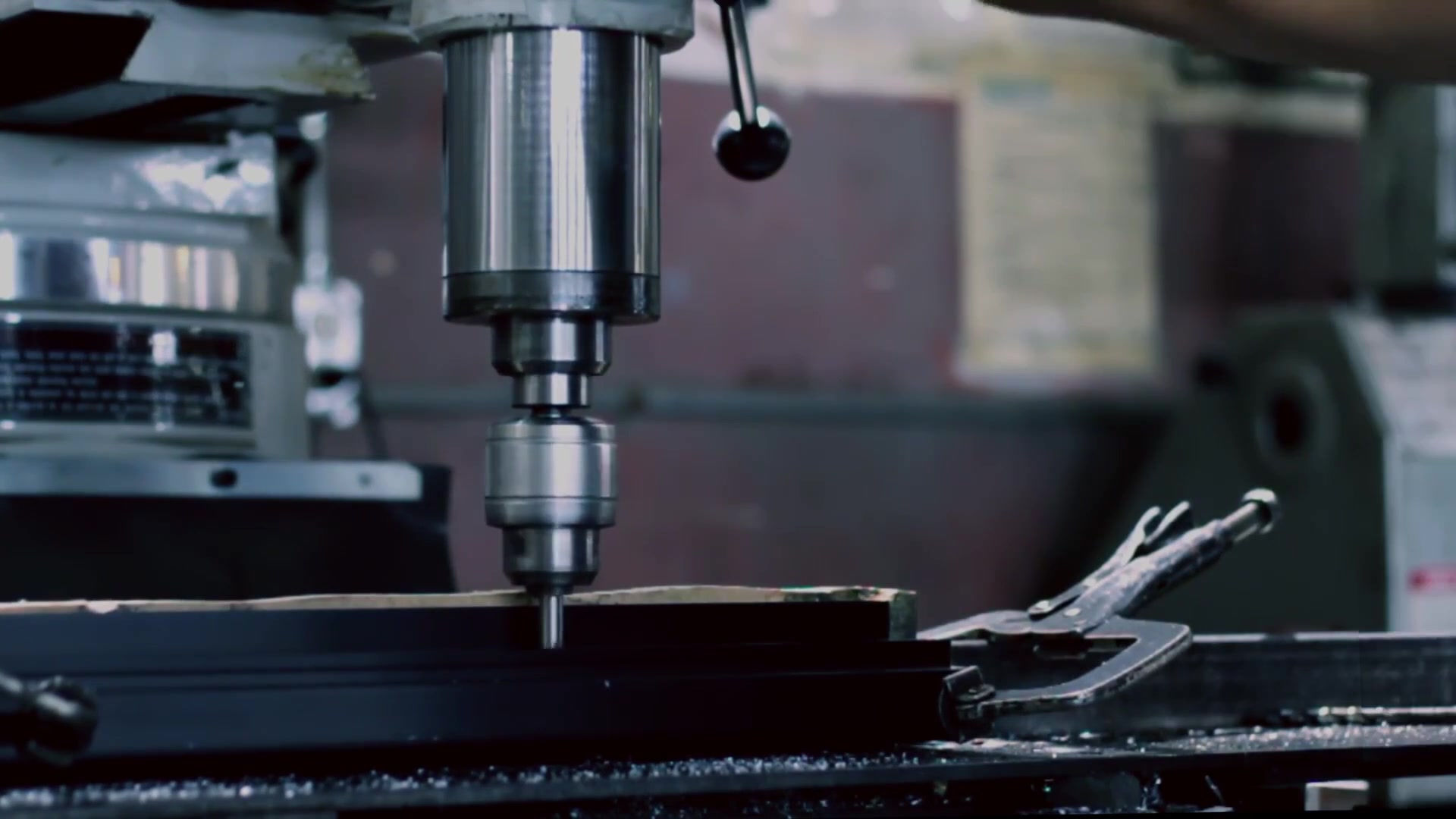
- Engineering Integration , USA , AGS-TECH Inc.
AGS-TECH, Inc. is globally recognized for its wide range of engineering integration, mechanical & optical & electronic & software integration capabilities. Инженерска интеграција - Механичка и оптичка и електронска и софтверска интеграција Ние не произведуваме само поединечни компоненти. Обезбедуваме и ИНЖЕНЕРСКА ИНТЕГРАЦИЈА - Механичка и оптичка и електронска и софтверска интеграција, склопување и тестирање. Со други зборови, ние можеме да ги произведуваме вашите компоненти и делови и можеме да ги подмонтираме или да ги составиме во целосни производи. Понатаму, можеме да интегрираме хардвер со софтвер и фирмвер, да вршиме тестирање и квалификација на вашите производи, можеме да ви етикетираме, пакуваме и да ви испраќаме како подготвени за продажба на вашите клиенти. Видовите услуги за инженерска интеграција што им ги нудиме на нашите клиенти долги години вклучуваат: - Инженерска интеграција и монтажа на механички компоненти изработени од метали, легури, пластика и еластомери (гуми). Примери на производи што ги произведувавме се склопови за макара, лежишта и запчаници, жици и тела произведени од нас за специфични апликации. - Инженерска интеграција и склопување на електрични и електронски компоненти како што се печатени плочки, склопови на жици и кабли, ладилници, куќиште и пакет на производи. Типични примери се напојувањата што ги произведувавме за нашите клиенти. - Инженерска интеграција и монтажа на оптички компоненти со механички, електрични и електронски компоненти. Типични примери се уреди за оптички сензори, уреди за оптичко тестирање. - Инженерска интеграција на оптички, електронски и механички хардвер со софтвер. Различни роботи и системи за автоматизација што ги направивме за нашите клиенти се примери за оваа група. Можеме да го напишеме кодот и да ги програмираме вашите вградени системи, роботи и опрема за автоматизација или ако веќе имате напишан код, можеме да го интегрираме со вашиот нов систем, да го дебагираме, да го измениме и дополнително да го подобриме вашиот код. За некои проекти успешно интегриравме софтвер кој не се наоѓа на полица или слободно достапен код во системите на нашите клиенти. Преземете ја брошурата за нашата ПРОГРАМА ЗА ПАРТНЕРСТВО ЗА ДИЗАЈН Ако сте најмногу заинтересирани за нашите инженерски и истражувачки и развојни способности наместо производствените способности, тогаш ве покануваме да ја посетите нашата веб-страница за инженерство http://www.ags-engineering.com CLICK Product Finder-Locator Service ПРЕТХОДНА СТРАНИЦА
- Non-Conventional Fabrication, ECM, EDM, PMC, Waterjet Machining,Plasma
Non-Conventional Fabrication, ECM, EDM, PMC, Waterjet Machining, Laser, Plasma, EBM Machining, Ultrasonic Machining, Soldering, Welding, Brazing,Special Bonding Неконвенционална изработка Прочитај повеќе ECM обработка, електрохемиска обработка, мелење Прочитај повеќе EDM обработка, глодање и мелење со електрично празнење Прочитај повеќе Хемиска обработка и фотохемиско бланирање Прочитај повеќе Воден млаз обработка и абразивна млазница и абразивна обработка и сечење Прочитај повеќе Ласерска обработка и сечење и LBM Прочитај повеќе Плазма обработка и сечење Прочитај повеќе Ултразвучна обработка и ротациона ултразвучна обработка и мелење со ултразвучно влијание Прочитај повеќе EBM Machining & Electron Beam Machining Прочитај повеќе Лемење и лемење и заварување Прочитај повеќе Adhesive Bonding & Sealing & Custom Mechanical Fastening and Assembly Among the major NON-CONVENTIONAL FABRICATION techniques we offer are Electrochemical Fabrication (also called Electrochemical Machining or ECM), Electrical Discharge Machining or EDM, Water Jet Cutting, Abrasive Water Jet Cutting (WJ, AWJ), Laser Beam Machining (LBM), Electron Beam Machining (EBM), Ultrasonic Machining (USM), Plasma Machining, Photochemical Machining (abbreviated as PCM or also called Chemical Etching, Metal Etching, Chemical Milling, Chemical Machining), Soldering, Brazing, Welding, Specialty Bonding and Pickling. Sometimes, it is easier and more economical to get the work done by some chemicals, pressurized water jet or even light rather than using traditional techniques such as machining and stamping. On the submenu pages, you can find a summary of each of these alternative non-conventional fabrication techniques we are offering you. Non-conventional fabrication is also referred to as non-traditional fabrication. What distinguishes convention and non-conventional fabrication techniques ? – Generally speaking, conventional fabrication involves changing the shape of a work piece using an implement made of a harder material. Machining hard materials using conventional methods may require significant time and energy and result in high costs. In addition, conventional machining may lead to excessive tool wear and loss of quality in the product owing to induced residual stresses during manufacture. Therefore, especially for hard alloys, non-conventional fabrication techniques may be better alternatives. Whereas conventional fabrication processes generally use mechanical energy (motion), non-conventional fabrication processes utilize other forms of energy. Main forms of energy non-conventional fabrication processes use are: Thermal, Chemical and Electrical Energy. There can be a large number of advantages of non-conventional fabrication techniques over conventional methods. Just to name a few, non-conventional fabrication may involve quieter operation and no sound pollution, such as is the case with Chemical Machining. In non-conventional fabrication, material removal may occur with or without chip formation. For example, in Electrochemical Machining, material removal occurs due to electrochemical dissolution at atomic levels. Non-conventional fabrication may involve lower waste of material due to low or no wear as compared to conventional fabrication. On the other hand, non-conventional fabrication methods do have some disadvantages such as higher capital costs and the need for skilled operators. Also, non-conventional fabrication methods are not suitable for every type of material economically. Here is a downloadable guide comparing conventional and non-conventional fabrication methods: - A Brief Comparison of Conventional and Non-Conventional Fabrication Methods Since we are the World’s most diverse Global Custom Manufacturer, Integrator, Consolidator and Outsourcing Partner; we see it as our duty to determine technically the most suitable and economically the most feasible fabrication technique for your needs. Available techniques involve our non-conventional fabrication methods among others. In order to contract us to manufacture your products, you do not need to be an expert in non-conventional fabrication methods or any other production techniques. We are here to assist and guide you in the right direction. All you need is to contact us and provide as much information as possible about your production needs. We will review your input and determine whether conventional or non-conventional fabrication techniques will be the best fit for your products. We will take into consideration many factors such as lead times, number of parts to be produced, costs, dimensional specifications of your parts and products, material properties and requirements and determine which non-conventional or conventional fabrication technique or techniques will be the best fit. For almost all fabrication techniques, whether it be conventional or non-conventional, we do use CAD/CAM and automated CNC machines as well as manual machines. Sometimes manual machinery is more suitable and practical while for high volume orders automated CNCs are deployed exclusively. We have prepared a brochure below which you can download as a reference source for frequently used mechanical engineering terms: - Download brochure for Common Mechanical Engineering Terms used by Designers and Engineers If you are mostly interested in our engineering and research & development capabilities instead of manufacturing capabilities, then we invite you to visit our engineering website http://www.ags-engineering.com (On our engineering website you can find details about our engineering services such as design, product development, consulting…etc.) КЛИКНЕТЕ Услуга за пронаоѓање на производи-локатор ПРЕТХОДНА СТРАНИЦА
- Fasteners including Anchors, Bolts, Nuts, Pin Fasteners, Rivets, Rods
Fasteners including Anchors, Bolts, Nuts, Pin Fasteners, Rivets, Rods, Screws, Sockets, Springs, Struts, Clamps, Washers, Weld Fasteners, Hangers from AGS-TECH Производство на сврзувачки елементи We manufacture FASTENERS under TS16949, ISO9001 quality management system according to international standards such as ASTM, SAE, ISO, DIN, MIL. All our fasteners are shipped along with material certifications and inspection reports. We supply off-shelf fasteners as well as custom manufacture fasteners according to your technical drawings in case you require something different or special. We do provide engineering services in designing and developing specialty fasteners for your applications. Some major types of fasteners we offer are: • Anchors • Bolts • Hardware • Nails • Nuts • Pin Fasteners • Rivets • Rods • Screws • Security Fasteners • Set Screws • Sockets • Springs • Struts, Clamps, and Hangers • Washers • Weld Fasteners - CLICK HERE to download catalog for rivet nuts, blind rivet, insert nuts, nylon locknuts, welded nuts, flange nuts - CLICK HERE to download additional info-1 on rivet nuts - CLICK HERE to download additional info-2 on rivet nuts - CLICK HERE to download catalog of our titanium bolts and nuts - CLICK HERE to download our catalog containing some popular off-shelf fasteners & hardware suitable for the electronics & computer industry. - Screws and Fasteners (Standard and Specialty) (Click on the blue text above to download the brochure. We can private label these for you. In other words, we can put your name and logo on these products) - Screws for Furniture and Wood (Click on the blue text above to download the brochure. We can private label these for you. In other words, we can put your name and logo on these products) - Screws for Window and Door (Click on the blue text above to download the brochure. We can private label these for you. In other words, we can put your name and logo on these products) - Private Label Hand Tools - Hand Tool Cabinets (Click blue text above to download catalog. We can private label these hand tools if you wish. In other words, we can put your company name, brand and label on them. This way you can promote your brand by reselling these to your customers. These hand tools can complement your product offerings in case you are selling fasteners) Our THREADED FASTENERS can be internally threaded as well as externally and come in various forms including: - ISO Metric Screw Thread - ACME - American National Screw Thread (Inch Sizes) - Unified National Screw Thread (Inch Sizes) - Worm - Square - Knuckle - Buttress Our threaded fasteners are available with Right- and Left-Handed Threads as well as with Single and Multiple Threads. Both Inch Threads as well as Metric Threads are available for fasteners. For Inch threaded fasteners external thread classes 1A, 2A and 3A as well as internal thread classes of 1B, 2B and 3B are available. These inch thread classes differ in the amount of allowances and tolerances. Classes 1A and 1B: These fasteners produce the loosest fit in assembly. They are used where ease of assembly and disassembly is needed such as stove bolts and other rough bolts and nuts. Classes 2A and 2B: These fasteners are fit for ordinary commercial products and interchangeable parts. Typical machine screws and fasteners are examples. Classes 3A and 3B: These fasteners are designed for exceptionally high-grade commercial products where a close fit is required. The cost of fasteners with threads in this class is higher. For metric threaded fasteners we have coarse-thread, fine-thread and a series of constant pitches available. Coarse-Thread Series: This series of fasteners are intended for use in general engineering work and commercial applications. Fine-Thread Series: This series of fasteners are for general use where a finer thread than the coarse-thread is needed. When compared to the coarse-thread screw, the fine-thread screw is stronger in both tensile and torsional strength and less likely to loosen under vibration. For the fasteners pitch and crest diameter, we have a number of tolerance grades as well as tolerance positions available. PIPE THREADS: Besides fasteners, we can machine threads on pipes according to the designation provided by you. Make sure to call out the size of thread on your technical blueprints for custom pipes. THREADED ASSEMBLIES: If you provide us threaded assembly drawings we can use our machines making fasteners for machining your assemblies. If you are unfamiliar with screw thread representations, we can prepare the blueprints for you. SELECTION OF FASTENERS: Product selection should ideally begin at the design stage. Please determine the objectives of your fastening job and consult us. Our fasteners experts will review your objectives and circumstances and recommend the right fasteners at the best in-place cost. To obtain the maximum machine-screw efficiency, a thorough knowledge of the properties of both screw and fastened materials is needed. Our fastener experts have this knowledge available to assist you. We will need from you some input such as the loads that the screws and fasteners must withstand, whether the load on the fasteners and screws is one of tension or shear, and whether the fastened assembly will be subject to impact shock or vibrations. Depending on all these and other factors such as ease of assembly, cost….etc., the recommended size, strength, head shape, thread type of the screws and fasteners will be proposed to you. Among our most common threaded fasteners are SCREWS, BOLTS and STUDS. MACHINE SCREWS: These fasteners have either fine or coarse threads and are available with a variety of heads. Machine screws can be used in tapped holes or with nuts. CAP SCREWS: These are threaded fasteners that join two or more parts by passing through a clearance hole in one part and screwing into a tapped hole in the other. Cap screws are also available with various head types. CAPTIVE SCREWS: These fasteners remain attached to the panel or parent material even when the mating part is disengaged. Captive screws meet military requirements, to prevent screws from being lost, for enabling faster assembly / disassembly and prevent damage from loose screws falling into moving parts and electrical circuits. TAPPING SCREWS: These fasteners cut or form a mating thread when driven into preformed holes. Tapping screws permit rapid installation, because nuts are not used and access is required from only one side of the joint. The mating thread produced by the tapping screw fits the screw threads closely, and no clearance is necessary. The close fit usually keeps the screws tight, even when vibration is present. Self-drilling tapping screws have special points for drilling and then tapping their own holes. No drilling or punching is needed for self-drilling tapping screws. Tapping screws are used in steel, aluminum (cast, extruded, rolled or die-formed) die castings, cast iron, forgings, plastics, reinforced plastics, resin-impregnated plywood and other materials. BOLTS: These are threaded fasteners that pass through clearance holes in assembled parts and thread into nuts. STUDS: These fasteners are shafts threaded at both ends and are used in assemblies. Two major types of studs are double-end stud and continuous stud. As for other fasteners, it is important to determine what kind of grade and finish (plating or coating) is the most suitable. NUTS: Both style-1 and style-2 metric nuts are available. These fasteners are used generally with bolts and studs. Hex nuts, hex-flanged nuts, hex-slotted nuts are popular. There are also variations within these groups. WASHERS: These fasteners perform many varied functions in mechanically fastened assemblies. Washers functions can be to span an oversized clearance hole, give better bearing for nuts and screw faces, distribute loads over larger areas, serve as locking devices for threaded fasteners, maintain spring resistance pressure, guard surfaces against marring, provide sealing function and much more. Many types of these fasteners are available such as flat washers, conical washers, helical spring washers, tooth-lock types, spring washers, special purpose types…etc. SETSCREWS: These are used as semipermanent fasteners to hold a collar, sheave, or gear on a shaft against rotational and translational forces. These fasteners are basically compression devices. Users should find the best combination of setscrew form, size, and point style that provides required holding power. Setscrews are categorized by their head style and point style desired. LOCKNUTS: These fasteners are nuts with special internal means for gripping threaded fasteners to prevent rotation. We can view locknuts basically as standard nuts, but with an added locking feature. Locknuts have many very useful application areas including tubular fastening, use of locknuts on spring clamps, use of locknut where assembly is subjected to vibratory or cyclic motions that could cause loosening, for spring mounted connections where the nut must remain stationary or is subject to adjustment. CAPTIVE OR SELF-RETAINING NUTS: This class of fasteners provide a permanent, strong, multiple-thread fastening on thin materials. Captive or self-retaining nuts are especially good when there are blind locations, and they can be attached without damaging finishes. INSERTS: These fasteners are special form nuts designed to serve the function of a tapped hole in blind or through-hole locations. Different types are available such as molded-in inserts, self-tapping inserts, external-internal threaded inserts, pressed-in inserts, thin material inserts. SEALING FASTENERS: This class of fasteners not only hold two or more parts together, but they can simultaneously offer sealing function for gases and liquids against leakage. We offer many types of sealing fasteners as well as custom designed sealed-joint constructions. Some popular products are sealing screws, sealing rivets, sealing nuts and sealing washers. RIVETS: Riveting is a fast, simple, versatile and economical method of fastening. Rivets are considered permanent fasteners as opposed to removable fasteners such as screws and bolts. Simply described, rivets are ductile metal pins inserted through holes in two or more parts and having the ends formed over to securely hold the parts. Since rivets are permanent fasteners, riveted parts cannot be disassembled for maintenance or replacement without knocking the rivet out and installing a new one in place for reassembly. The type of rivets available are large and small rivets, rivets for aerospace equipment, blind rivets. As with all fasteners we sell, we do help our customers in the design and product selection process. From the type of rivet suitable for your application, to the speed of installation, in-place costs, spacing, length, edge distance and more, we are capable to assist you in your design process. Reference Code: OICASRET-GLOBAL, OICASTICDM КЛИКНЕТЕ Услуга за пронаоѓање на производи-локатор ПРЕТХОДНА СТРАНИЦА
- Adhesive Bonding - Adhesives - Sealing - Fastening - Joining
Adhesive Bonding - Adhesives - Sealing - Fastening - Joining Nonmetallic Materials - Optical Contacting - UV Bonding - Specialty Glue - Epoxy - Custom Assembly Лепливо врзување и запечатување и прилагодено механичко прицврстување и склопување Among our other most valuable JOINING techniques are ADHESIVE BONDING, MECHANICAL FASTENING and ASSEMBLY, JOINING NONMETALLIC MATERIALS. We dedicate this section to these joining and assembly techniques because of their importance in our manufacturing operations and the extensive content related to them. ADHESIVE BONDING: Did you know that there are specialized epoxies that can be used for almost hermetic level sealing ? Depending on the level of sealing you require, we will choose or formulate a sealant for you. Also do you know that some sealants can be heat cured whereas others require only a UV light to be cured ? If you explain us your application, we can formulate the right epoxy for you. You may require something that is bubble free or something that matches the thermal coefficient of expansion of your mating parts. We have it all ! Contact us and explain your application. We will then choose the most suitable material for you or custom formulate a solution for your challenge. Our materials come with inspection reports, material data sheets and certification. We are capable to assemble your components very economically and ship you completed and quality inspected products. Adhesives are available to us in various forms such as liquids, solutions, pastes, emulsions, powder, tape and films. We use three basic types of adhesives for our joining processes: -Natural Adhesives -Inorganic Adhesives -Synthetic Organic Adhesives For load-bearing applications in manufacturing and fabrication we use adhesives with high cohesive strength, and they are mostly synthetic organic adhesives, which may be thermoplastics or thermosetting polymers. Synthetic organic adhesives are our most important category and can be classified as: Chemically Reactive Adhesives: Popular examples are silicones, polyurethanes, epoxies, phenolics, polyimides, anaerobics like Loctite. Pressure Sensitive Adhesives: Common examples are natural rubber, nitrile rubber, polyacrylates, butyl rubber. Hot Melt Adhesives: Examples are thermoplastics like ethylene-vinyl-acetate copolymers, polyamides, polyester, polyolefins. Reactive Hot Melt Adhesives: They have a thermoset portion based on urethane’s chemistry. Evaporative / Diffusion Adhesives: Popular ones are vinyls, acrylics, phenolics, polyurethanes, synthetic and natural rubbers. Film and Tape Type Adhesives: Examples are nylon-epoxies, elastomer-epoxies, nitrile-phenolics, polyimides. Delayed Tack Adhesives: These include polyvinyl acetates, polystyrenes, polyamides. Electrically and Thermally Conductive Adhesives: Popular examples are epoxies, polyurethanes, silicones, polyimides. According to their chemistries adhesives we use in manufacturing can be classified as: - Epoxy based adhesive systems: High strength and high temperature endurance as high as 473 Kelvin are characteristic of these. Bonding agents in sand mold castings are this type. - Acrylics: These are suitable for applications that involve contaminated dirty surfaces. - Anaerobic adhesive systems: Curing by oxygen deprivation. Hard and brittle bonds. - Cyanoacrylate: Thin bond lines with setting times under 1 minute. - Urethanes: We use them as popular sealants with high toughness and flexibility. - Silicones: Well known for their resistance against moisture and solvents, high impact and peel strength. Relatively long curing times of up to a few days. To optimize the properties in adhesive bonding, we may combine several adhesives. Examples are epoxy-silicon, nitrile-phenolic combined adhesive systems. Polyimides and polybenzimidazoles are used in high-temperature applications. Adhesive joints withstand shear, compressive, and tensile forces pretty well but they may easily fail when subjected to peeling forces. Therefore, in adhesive bonding, we must consider the application and design the joint accordingly. Surface preparation is also of critical importance in adhesive bonding. We clean, treat and modify surfaces to increase the strength and reliability of interfaces in adhesive bonding. Using special primers, wet and dry etching techniques such as plasma cleaning are among our common methods. An adhesion promoting layer such as a thin oxide may improve adhesion in some applications. Increasing surface roughness may also be beneficial prior to adhesive bonding but needs to be well controlled and not exaggerated because excessive roughness can result in trapping of air and therefore a weaker adhesively bonded interface. We use nondestructive methods for testing the quality and strength of our products after adhesive bonding operations. Our techniques include methods such as acoustic impact, IR detection, ultrasonic testing. Advantages of adhesive bonding are: -Adhesive bonding can provide structural strength, sealing and insulation function, suppression of vibration and noise. -Adhesive bonding can eliminate localized stresses at the interface by eliminating the need for joining using fasteners or welding. -Generally no holes are needed for adhesive bonding, and therefore external appearance of components is unaffected. -Thin and fragile parts can be adhesively joined without damage and without significant increase in weight. -Adhesive joining can be used to bond parts made of very different materials with significantly different sizes. -Adhesive bonding can be used on heat sensitive components safely due to low temperatures involved. However some disadvantages do exist for adhesive bonding and our customers should consider these prior to finalizing their designs of joints: -Service temperatures are relatively low for adhesively joint components -Adhesive bonding may require long bonding and curing times. -Surface preparation is needed in adhesive bonding. -Especially for large structures it may be difficult to test adhesively bonded joints nondestructively. -Adhesive bonding may pose reliability concerns in the long term due to degradation, stress corrosion, dissolution….and the like. One of our outstanding products is ELECTRICALLY CONDUCTIVE ADHESIVE, which can replace lead-based solders. Fillers such as silver, aluminum, copper, gold make these pastes conductive. Fillers can be in the form of flakes, particles or polymeric particles coated with thin films of silver or gold. Fillers can also improve thermal conductivity besides electrical. Let us continue with our other joining processes used in manufacturing products. MECHANICAL FASTENING and ASSEMBLY: Mechanical fastening offers us ease of manufacturing, ease of assembly and disassembly, ease of transportation, ease of parts replacement, maintenance and repair, ease in design of movable and adjustable products, lower cost. For fastening we use: Threaded Fasteners: Bolts, screws and nuts are examples of these. Depending on your application, we can provide you specially designed nuts and lock washers for dampening vibration. Riveting: Rivets are among our most common methods of permanent mechanical joining and assembly processes. Rivets are placed in holes and their ends are deformed by upsetting. We perform assembly using riveting at room temperature as well as at high temperatures. Stitching / Stapling / Clinching: These assembly operations are widely used in manufacturing and are basically the same as is used on papers and cardboards. Both metallic and nonmetallic materials can be joined and assembled quickly without need to predrill holes. Seaming: An inexpensive fast joining technique we use widely in manufacturing of containers and metal cans. It is based on folding two thin pieces of material together. Even airtight and watertight seams are possible, especially if seaming is performed jointly with using sealants and adhesives. Crimping: Crimping is a joining method where we do not use fasteners. Electrical or fiber optic connectors are sometimes installed using crimping. In high volume manufacturing, crimping is an indispensible technique for fast joining and assembly of both flat and tubular components. Snap-in Fasteners: Snap fits are also an economical joining technique in assembly and manufacturing. They permit quick assembly and disassembly of components and are a good fit for household products, toys, furniture among others. Shrink and Press Fits: Another mechanical assembly technique, namely shrink fitting is based on the principle of differential thermal expansion and contraction of two components, whereas in press fitting one component is forced over another resulting in good joint strength. We use shrink fitting widely in the assembly and manufacturing of cable harness, and mounting gears and cams on shafts. JOINING NONMETALLIC MATERIALS: Thermoplastics can be heated and melted at the interfaces to be joined and by applying pressure adhesive joining can be accomplished by fusion. Alternatively thermoplastic fillers of the same type may be used for the joining process. Joining of some polymers such as polyethylene may be difficult due to oxidation. In such cases, an inert shielding gas like nitrogen may be used against oxidation. Both external as well as internal heat sources can be used in adhesive joining of polymers. Examples of external sources we commonly use in adhesive joining of thermoplastics are hot air or gases, IR radiation, heated tools, lasers, resistive electrical heating elements. Some of our internal heat sources are ultrasonic welding and friction welding. In some assembly and manufacturing applications we use adhesives for bonding polymers. Some polymers such as PTFE (Teflon) or PE (Polyethylene) have low surface energies and therefore a primer is first applied prior to completing the adhesive bonding process with a suitable adhesive. Another popular technique in joining is the “Clearweld Process” where a toner is first applied to the polymer interfaces. A laser is then directed at the interface, but it does not heat the polymer, but does heat the toner. This makes it possible to heat only well-defined interfaces resulting in localized welds. Other alternative joining techniques in the assembly of thermoplastics are using fasteners, self-tapping screws, integrated snap-fasteners. An exotic technique in manufacturing and assembly operations is embedding tiny micron-sized particles into the polymer and using high-frequency electromagnetic field to inductively heat and melt it at the interfaces to be joined. Thermoset materials on the other hand, do not soften or melt with increasing temperatures. Therefore, adhesive joining of thermoset plastics are usually carried out using threaded or other molded-in inserts, mechanical fasteners and solvent bonding. Regarding joining and assembly operations involving glass and ceramics in our manufacturing plants, here are a few common observations: In cases where a ceramic or glass have to be joined with difficult-to-bond materials, the ceramic or glass materials are frequently coated with a metal that bonds itself easily to them, and then joined to the difficult-to-bond material. When ceramic or glass has a thin metal coating it can be more readily brazed to metals. Ceramics are sometimes joined and assembled together during their shaping process while still hot, soft and tacky. Carbides can be more easily brazed to metals if they have as their matrix material a metal binder such as cobalt or nickel-molybdenum alloy. We braze carbide cutting tools to steel toolholders. Glasses bond well to each other and metals when hot and soft. Information on our facility producing ceramic to metal fittings, hermetic sealing, vacuum feedthroughs, high and ultrahigh vacuum and fluid control components can be found here: Brazing Factory Brochure Private Label Epoxy Solutions for Construction, Electrical, Industrial Assembly (Download brochure by clicking on blue text. We can put your name, label, logo on these epoxies if you wish) КЛИКНЕТЕ Услуга за пронаоѓање на производи-локатор ПРЕТХОДНА СТРАНИЦА
- PRIVATE & WHITE LABEL PRODUCT CATALOGS
PRIVATE & WHITE LABEL PRODUCT CATALOGS AGS-TECH, Inc. е ваш Производител и добавувач на приватна и бела етикета. Од нас можете да набавите производи со вашиот бренд, лого и етикета. Многу од нашите готови производи може да ви бидат испорачани со името на вашата марка на нив, за да можете веднаш да започнете со продажба и промовирање на вашиот бренд. Каталози и брошури за производи со приватна и бела етикета Подолу можете да кликнете и преземете некои од нашите каталози на производи со приватна етикета. Можете да ги изберете овие производи кои не се достапни на полица, кажете ни кои би сакале да ги купите, а ние ќе ги испечатиме вашето име, етикета, логото на нив. Дополнително, можеме да ги пакуваме по желба со вашето име на нив. Кога ќе ги продавате, вашите клиенти ќе го видат само вашето име и бренд на нив. Да повториме, ова се готови производи. Во случај да сакате да ги измениме овие за вас или да го произведеме вашиот уникатен дизајн, ние исто така го правиме тоа. Please click on highlighted text below to download respective catalogs of some products we can supply you with your Private Label or White Label. Our private label products are much more than these. Here we listed some of them. The catalogs and brochures below are in alphabetical order: - Abrasives - Abrasives (Private Label Ordering Instructions Guide) - Aerosols and Sprays - Auto Glass Repair and Replacement Systems - Barcode and Fixed Mount Scanners - RFID Products - Mobile Computers - Micro Kiosks OEM Technology - Barcode Scanners - Batteries - LiFePO4 - Brazing Machines - Cleanroom Consumables and Apparel - Drill Bits - Epoxy Solutions for Construction, Electrical, Industrial Assembly - EV Chargers - Fixed Industrial Scanners - Flash Storage for Embedded Industrial Applications - Folding Utility Knife - Gauges, Filters, Regulators, Temperature Instruments - Hand Tools for Every Industry - Hand Tools - Hand Tool Cabinets - Helium Leak Tester - Hose Crimping Machines - Hose-Cut-Off-Skive-Machine - Hose Endforming Machines - Hydraulic Reservoirs - Industrial Filters - Kiosk Systems - Kiosk Systems Accessories Guide - LED Lighting Products (OEM, ODM, Private Label) - Low-Voltage Cables - Low-Voltage Cables & Accessories for AV - DataCom - CATV - Security - LAN - Electrical - Measuring Tapes Combo - Medical Endoscopes and Visualization Systems - Mobile Computers for Enterprises - Nano Surface Protection Car Care Products - Nano Surface Protection Industrial Products - Nano Surface Protection Marine Products - Nano Surface Protection Products - Pneumatic Air Blow Guns - Pneumatic Compressed Air Hoses Fittings - Pneumatic Compressed Air Tools - Pneumatic Couplings, Plugs and Nipples - Power Tool Accessories - Drill Bits - Cutting Grinding Polishing Disks - Hole Saws - Jig Saw Blades....etc. - Power Tools for Every Industry - Printers for Barcode Scanners and Mobile Computers - Process Automation Solutions - Ratcheting Screwdriver - RFID Readers - Scanners - Encoders - Printers - Screwdriver 6 in 1 - Screws and Fasteners (Standard and Specialty) - Screws for Furniture and Wood - Screws for Window and Door - Sensors & Analytical Measurement Systems for Liquid Analysis - Sensors & Analytical Measurement Systems for Optical OEM Applications in Liquid Analysis - Sensors & Analytical Measurement Systems for pH Testing - Servo C-Frame Utility Press - Tapes for Every Application - Taps - Cutting Tools - Tube Bending Machines - Valves for Liquids and Gas Ние сме AGS-TECH Inc., ваш единствен извор за производство и изработка и инженерство и аутсорсинг и консолидација. Ние сме најразновидниот инженерски интегратор во светот кој ви нуди сопствено производство, подсклопување, склопување на производи и инженерски услуги.
- Camera Systems & Components, Optic Scanner, Optical Readers, CCD
Camera Systems - Components - Optic Scanner - Optical Readers - Imaging System - CCD - Optomechanical Systems - IR Cameras Производство и склопување приспособени системи за камера AGS-TECH offers: • Camera systems, camera components and custom camera assemblies • Custom designed and manufactured optical scanners, readers, optical security product assemblies. • Precision optical, opto-mechanical and electro-optical assemblies integrating imaging and nonimaging optics, LED lighting, fiber optics and CCD cameras • Among the products our optical engineers have developed are: - Omni-directional periscope and camera for surveillance and security applications. 360 x 60º field of view high resolution image, no stitching required. - Inner cavity wide angle video camera - Super slim 0.6 mm diameter flexible video endoscope. All medical video couplers fit over standard endoscope eyepieces and are completely sealed and soakable. For our medical endoscope and camera systems, please visit: http://www.agsmedical.com - Video camera and coupler for semi-rigid endoscope - Eye-Q Videoprobe. Non-contact zoom videoprobe for coordinate measuring machines. - Optical spectrograph & IR imaging system (OSIRIS) for ODIN satellite. Our engineers worked on the flight unit assembly, alignment, integration and test. - Wind imaging interferometer (WINDII) for NASA upper atmosphere research satellite (UARS). Our engineers worked on consulting on assembly, integration and test. WINDII performance and operational lifetime far exceeded the design goals and requirements. Depending on your application, we will determine what dimensions, pixel count, resolution, wavelength sensitivity your camera application requires. We can build systems for you suitable for infrared, visible and other wavelengths. Contact us today to find out more. Dowload brochure for our DESIGN PARTNERSHIP PROGRAM Developing a customized camera system can take relatively longer lead times and cost more as compared to ready-to-use systems. Therefore please click on the blue links below to check whether any of our ready-to-use products fit your application: Barcode and Fixed Mount Scanners - RFID Products - Mobile Computers - Micro Kiosks OEM Technology (We private label these with your brand name and logo if you wish) Barcode Scanners (We private label these with your brand name and logo if you wish) Fixed Industrial Scanners (We private label these with your brand name and logo if you wish) Hikrobot Machine Vision Products Hikrobot Smart Machine Vision Products Hikrobot Machine Vision Standard Products Hikvision Logistic Vision Solutions Private Label Medical Endoscopes and Visualization Systems (We can put your company name and logo on these) Also make sure to download our comprehensive electric & electronic components catalog for off-shelf products by CLICKING HERE. КЛИКНЕТЕ Услуга за пронаоѓање на производи-локатор ПРЕТХОДНА СТРАНИЦА
- Computer Storage Devices, Disk Array, NAS Array, Storage Area Network
Computer Storage Devices - Disk Array - NAS Array - Storage Area Network - SAN - Utility Storage Arrays - AGS-TECH Inc. Уреди за складирање, низи на дискови и системи за складирање, SAN, NAS A STORAGE DEVICE or also known as STORAGE MEDIUM is any computing hardware that is used for storing, porting and extracting data files and objects. Storage devices can hold and store information temporarily as well as permanently. They can be internal or external to a computer, to a server or to any similar computing device. Our focus is on DISK ARRAY which is a hardware element that contains a large group of hard disk drives (HDDs). Disk arrrays may contain several disk drive trays and have architectures improving speed and increasing data protection. A storage controller runs the system, which coordinates activity within the unit. Disk arrays are the backbone of modern storage networking environments. A disk array is a DISK STORAGE SYSTEM which contains multiple disk drives and is differentiated from a disk enclosure, in that an array has cache memory and advanced functionality such as RAID and virtualization. RAID stands for Redundant Array of Inexpensive (or Independent) Disks and employs two or more drives to improve performance and fault tolerance. RAID enables the storage of data in multiple places to protect the data against corruption and to serve it to users faster. Click on the blue highlighted text to download catalogs and brochures: Private Label Flash Storage for Embedded Industrial Applications (We can put your name, logo, brand on these.........) To choose a suitable Industrial Grade Storage Device for your project, please go to our industrial computer store by CLICKING HERE. Dowload brochure for our DESIGN PARTNERSHIP PROGRAM Components of a typical disk array include: - Disk array controllers - Cache memories - Disk enclosures - Power supplies Generally disk arrays provide increased availability, resiliency and maintainability by using additional, redundant components such as controllers, power supplies, fans, etc., to the degree that all single points of failure are eliminated from the design. These components are most of the time hot-swappable. Typically, disk arrays are divided into categories: NETWORK ATTACHED STORAGE (NAS) ARRAYS : NAS is a dedicated file storage device that provides local-area network (LAN) users with centralized, consolidated disk storage through a standard Ethernet connection. Each NAS device is connected to the LAN as an independent network device and assigned an IP address. Its main advantage is that network storage is not limited to the storage capacity of a computing device or the number of disks in a local server. NAS products can generally hold enough disks to support RAID, and multiple NAS appliances can be attached to the network for storage expansion. STORAGE AREA NETWORK (SAN) ARRAYS : They contain one or more disk arrays that function as the repository for the data which is moved in and out of the SAN. Storage arrays connect to the fabric layer with cables running from the devices in the fabric layer to the GBICs in the ports on the array. There are mainly two types of storage area network arrays, namely modular SAN arrays and monolithic SAN arrays. Both of them use built-in computer memory to speed up and cache access to slow disk drives. The two types use memory cache differently. Monolithic arrays generally have more cache memory compared to modular arrays. 1.) MODULAR SAN ARRAYS : These have fewer port connections, they store less data and connect to fewer servers compared to monolithic SAN arrays. They make it possible for the user such as small companies to start small with a few disk drives and to increase the number as storage needs grow. They have shelves for holding disk drives. If connected to only a few servers, modular SAN arrays can be very fast and offer companies a flexibility. Modular SAN arrays fit into standard 19” racks. They generally use two controllers with separate cache memory in each and mirror the cache between the controllers to prevent data loss. 2.) MONOLITHIC SAN ARRAYS : These are big collections of disk drives in data centers. They can store much more data compared to modular SAN arrays and generally connect to mainframes. Monolithic SAN arrays have many controllers that can share direct access to fast global memory cache. Monolithic arrays generally have more physical ports to connect to storage area networks. Thus more servers can use the array. Typically monolithic arrays are more valuable and have superior built-in redundancy and reliability. UTILITY STORAGE ARRAYS : In utility storage service model, a provider offers storage capacity to individuals or organizations on a pay-per-use basis. This service model is also referred to as storage on demand. This facilitates efficient use of resources and reduces cost. This can be more cost effective to companies by eliminating the need to purchase, manage and maintain infrastructures that meet peak requirements which may be beyond the needed capacity limits. STORAGE VIRTUALIZATION : This uses virtualization to enable better functionality and more advanced features in computer data storage systems. Storage virtualization is the apparent pooling of data from several same-type or different types of storage devices into what appears to be a single device managed from a central console. It helps storage administrators perform backup, archiving and recovery more easily and faster by overcoming the complexity of a storage area network (SAN). This can be achieved by implementing virtualization with software applications or using hardware and software hybrid appliances. КЛИКНЕТЕ Услуга за пронаоѓање на производи-локатор PREVIOUS PAGE
- AGS-TECH Inc Customer References - Custom Manufacturing & Integration
AGS-TECH Inc Customer References - We have many loyal customers satisfied with our global custom manufacturing & engineering integration services Референци на клиентите AGS-TECH, Inc. опслужува домашни и меѓународни клиенти речиси две децении. Многу од нашите клиенти долги години ги доставуваат производствените операции, компоненти, делови, склопови и готови производи од нас. Контактирајте не за референци на клиентите. PLEASE CLICK HERE TO READ TESTIMONIALS AND FEEDBACK FROM SOME OF OUR CUSTOMERS ПРЕТХОДНА СТРАНИЦА
- Rubber and Elastomer Molds, Molding, Rubber Injection Molding, Toys
Rubber and Elastomer Molds & Molding, Rubber Injection Molding, Rubber Toy Manufacturing Калапи и калапи од гума и еластомер Дел од калап со вбризгување на гума склопен со други метални делови. Ние ги правиме калапите и алатките за производство на ваши сопствени делови. Механички склоп со гумена компонента обликувана со инјектирање. Целото склопување беше произведено од AGS-TECH Inc. Гумени играчки произведени од AGS-TECH Inc. Делови по мерка изработени од голем избор на гумени материјали Прилагодено гумено обликување на автомобилски душеци за еден од нашите клиенти - AGS-TECH Inc - Посетете не на www.agstech.net Лиени гумени компоненти собрани во спортски производи. Сите компоненти произведени и составени од AGS-TECH Inc. Rubber Belts Manufacturing by AGS-TECH Inc. Производство на О-прстен во AGS-TECH Inc. Лиен О-прстен комплети Екструдирани гумени делови од EPDM - NBR - CR - SILICONE - PVC - TPE - TPV Екструзија на гума од EPDM - NBR - CR - SILICONE - PVC - TPE - TPV изработена од AGS-TECH Екструзија од EPDM - NBR - CR - SILICONE - PVC - TPE - TPV Лиени гумени делови од EPDM - NBR - CR - SILICONE - PVC - TPE - TPV Екструдирана гума изработена од EPDM - NBR - CR - SILICONE - PVC - TPE - TPV ПРЕТХОДНА СТРАНИЦА
- Microwave Components & Subassembly, Microwave Circuits, RF Transformer
Microwave Components - Subassembly - Microwave Circuits - RF Transformer - LNA - Mixer - Fixed Attenuator - AGS-TECH Производство и склопување на компоненти и системи за микробранови We manufacture and supply: Microwave electronics including silicon microwave diodes, dot touch diodes, schottky diodes, PIN diodes, varactor diodes, step recovery diodes, microwave integrated circuits, splitters/combiners, mixers, directional couplers, detectors, I/Q modulators, filters, fixed attenuators, RF transformers, simulation phase shifters, LNA, PA, switches, attenuators, and limiters. We also custom manufacture microwave subassemblies and assemblies according to users' requirements. Please download our microwave components and systems brochures from the links below: Antenna Brochure for 5G - LTE 4G - LPWA 3G - 2G - GPS - GNSS - WLAN - BT - Combo - ISM Barcode and Fixed Mount Scanners - RFID Products - Mobile Computers - Micro Kiosks OEM Technology (We private label these with your brand name and logo if you wish) Barcode Scanners (We private label these with your brand name and logo if you wish) Microwave Flexible Cable Assembly Microwave and Milimeter Wave Test Accessories Brochure (Cable assemblies, VNA Test Assemblies, Mechanical Calibration Kits, RF Coaxial Adapters, Test Port Adapters, DC Blocks, NMD Connectors....etc.) Microwave Waveguides - Coaxial Components - Milimeterwave Antennas (Straight Waveguide, Waveguide Bend, Waveguide to Coaxial Adapter, Directional Couplers, Waveguide Tee, Circulators, Isolators......etc.) Printers for Barcode Scanners and Mobile Computers (We private label these with your brand name and logo if you wish) RF and Microwave Components (Broadband 90/180 Degree Hybrid and Coupler, Broadband Power Divider, Filter, RF switch, Broadband Amplifier, Broadband Frequency Synthesizer) RFID Readers - Scanners - Encoders - Printers (We private label these with your brand name and logo if you wish) Soft Ferrites - Cores - Toroids - EMI Suppression Products - RFID Transponders and Accessories Brochure Dowload brochure for our DESIGN PARTNERSHIP PROGRAM Microwaves are electromagnetic waves with wavelengths ranging from 1 mm to 1 m, or frequencies between 0.3 GHz and 300 GHz.The microwave range includes ultra-high frequency (UHF) (0.3–3 GHz), super high frequency (SHF) (3–30 GHz), and extremely high frequency (EHF) (30–300 GHz) signals. Uses of microwave technology: COMMUNICATION SYSTEMS: Before the invention of fiber optic transmission technology, most long distance telephone calls were carried via microwave point-to-point links through sites like the AT&T Long Lines. Starting in the early 1950s, frequency division multiplexing was used to send up to 5,400 telephone channels on each microwave radio channel, with as many as ten radio channels combined into one antenna for the hop to the next site, that was up to 70 km away. Wireless LAN protocols, such as Bluetooth and the IEEE 802.11 specifications, also use microwaves in the 2.4 GHz ISM band, although 802.11a uses ISM band and U-NII frequencies in the 5 GHz range. Licensed long-range (up to about 25 km) Wireless Internet Access services can be found in many countries in the 3.5–4.0 GHz range (not in the USA however). Metropolitan Area Networks: MAN protocols, such as WiMAX (Worldwide Interoperability for Microwave Access) based in the IEEE 802.16 specification. The IEEE 802.16 specification was designed to operate between 2 to 11 GHz frequencies. The commercial implementations are in the 2.3GHz, 2.5 GHz, 3.5 GHz and 5.8 GHz frequency ranges. Wide Area Mobile Broadband Wireless Access: MBWA protocols based on standards specifications such as IEEE 802.20 or ATIS/ANSI HC-SDMA (e.g. iBurst) are designed to operate between 1.6 and 2.3 GHz to give mobility and in-building penetration characteristics similar to mobile phones but with much much greater spectral efficiency. Some of the lower microwave frequency spectrum is used on Cable TV and Internet access on coaxial cable as well as broadcast television. Also some mobile phone networks, like GSM, also use lower microwave frequencies. Microwave radio is used in broadcasting and telecommunication transmissions because, due to their short wavelength, highly directive antennas are smaller and therefore more practical than they would be at lower frequencies (longer wavelengths). There is also more bandwidth in the microwave spectrum than in the rest of the radio spectrum; the usable bandwidth below 300 MHz is less than 300 MHz while many GHz can be used above 300 MHz. Typically, microwaves are used in television news to transmit a signal from a remote location to a television station in a specially equipped van. The C, X, Ka, or Ku Bands of the microwave spectrum are used in the operation of most satellite communications systems. These frequencies allow large bandwidth while avoiding the crowded UHF frequencies and staying below the atmospheric absorption of EHF frequencies. Satellite TV either operates in the C band for the traditional large dish Fixed Satellite Service or Ku band for Direct Broadcast Satellite. Military communication systems run primarily over X or Ku Band links, with Ka band being used for Milstar. REMOTE SENSING: Radars use microwave frequency radiation to detect the range, speed, and other characteristics of remote objects. Radars are widely used for applications including air traffic control, navigation of ships, and traffic speed limit control. Besides ultrasonic decices, sometimes Gunn diode oscillators and waveguides are used as motion detectors for automatic door openers. Much of radio astronomy uses microwave technology. NAVIGATION SYSTEMS: Global Navigation Satellite Systems (GNSS) including the American Global Positioning System (GPS), the Chinese Beidou and the Russian GLONASS broadcast navigational signals in various bands between about 1.2 GHz and 1.6 GHz. POWER: A microwave oven passes (non-ionizing) microwave radiation (at a frequency near 2.45 GHz) through food, causing dielectric heating by absorption of energy in the water, fats and sugar contained in the food. Microwave ovens became common following development of inexpensive cavity magnetrons. Microwave heating is widely used in industrial processes for drying and curing products. Many semiconductor processing techniques use microwaves to generate plasma for purposes such as reactive ion etching (RIE) and plasma-enhanced chemical vapor deposition (PECVD). Microwaves can be used to transmit power over long distances. NASA worked in the 1970s and early 1980s to research the possibilities of using Solar Power Satellite (SPS) systems with large solar arrays that would beam power down to the Earth's surface via microwaves. Some light weaponry uses millimeter waves to heat a thin layer of human skin to an intolerable temperature to make the targeted person move away. A two-second burst of the 95 GHz focused beam heats the skin to a temperature of 130 °F (54 °C) at a depth of 1/64th of an inch (0.4 mm). The United States Air Force and Marines use this type of Active Denial System. If your interest is in engineering and research & development, please visit our engineering site http://www.ags-engineering.com КЛИКНЕТЕ Услуга за пронаоѓање на производи-локатор ПРЕТХОДНА СТРАНИЦА
