

Global Custom Manufacturer, Integrator, Consolidator, Outsourcing Partner for a Wide Variety of Products & Services.
We are your one-stop source for manufacturing, fabrication, engineering, consolidation, integration, outsourcing of custom manufactured and off-shelf products & services. We also private label / white label your products with your brand name if you wish.
Choose your Language
-
Custom Manufacturing of Parts, Components, Assemblies, Finished Products, Machines and Industrial Equipment
-
Domestic & Global Contract Manufacturing
-
Manufacturing Outsourcing
-
Domestic, Global Procurement of Industrial Products
-
Private labeling / White Labeling your Products with your Brand Name
-
Product Finding & Locating Services
-
Global Design and Channel Partnership
-
Engineering Integration
-
Engineering Services
-
Global Consolidation, Warehousing, Logistics
Search Results
164 results found with an empty search
- Chemical Physical Environmental Analyzers, NDT, Nondestructive Testing
Chemical Physical Environmental Analyzers, NDT, Nondestructive Testing, Analytical Balance, Chromatograph, Mass Spectrometer, Gas Analyzer, Moisture Analyzer Chemical, Physical, Environmental Analyzers The industrial CHEMICAL ANALYZERS we provide are: CHROMATOGRAPHS, MASS SPECTROMETERS, RESIDUAL GAS ANALYZERS, GAS DETECTORS, MOISTURE ANALYZER, DIGITAL GRAIN AND WOOD MOISTURE METERS, ANALYTICAL BALANCE The industrial PHYSICAL ANALYSIS INSTRUMENTS we offer are: SPECTROPHOTOMETERS, POLARIMETER, REFRACTOMETER, LUX METER, GLOSS METERS, COLOR READERS, COLOR DIFFERENCE METER , DIGITAL LASER DISTANCE METERS, LASER RANGEFINDER, ULTRASONIC CABLE HEIGHT METER, SOUND LEVEL METER, ULTRASONIC DISTANCE METER , DIGITAL ULTRASONIC FLAW DETECTOR , HARDNESS TESTER , METALLURGICAL MICROSCOPES , SURFACE ROUGHNESS TESTER , ULTRASONIC THICKNESS GAUGE , VIBRATION METER , TACHOMETER . and others...... For the highlighted products, please visit our related pages by clicking on the corresponding colored text above. The ENVIRONMENTAL ANALYZERS we provide are: TEMPERATURE & HUMIDITY CYCLING CHAMBERS, ENVIRONMENTAL TESTING CHAMBERS, LIQUID ANALYSIS & TEST SYSTEMS. Click on Colored Text to Download Catalogs below. Choose the brand and model number of your interest and let us know whether you need brand new, or refurbished / used equipment: AMETEK-LLOYD Instruments Materials Testing (Versatile Materials Testing Equipment, Universal Test Machines, Tensile Strength, Compressibility, Hardness, Elasticity, Peeling, Adhesion...etc.) ELCOMETER Inspection Equipment Catalog ( Physical Test Equipment , Gloss & Reflectance , Colour Measurement , Fineness Of Grind/Dispersion , Density & Specific Gravity , Viscosity & Flow Measurement , Film Application & Test Charts , Drying Time & Permeability , Washability & Abrasion , Hardness & Scratch Resistance , Elasticity, Bend & Impact Testers , Flash Point, Concrete Inspection Equipment ) FLUKE Test Tools Catalog (includes Indoor Air Quality Tools, Air Meter, Airflow Meter, Temperature-Humidity Meter, Particle Counter, Carbon Monoxide Meters) HAIDA Anti-Yellowing Aging Test Chamber HAIDA Color Assessment Cabinet HAIDA IPX1&X2 Water Drip Test Chamber HAIDA Rapid-Rate Thermal Cycle Chamber HAIDA Salt Corrosion Spray Test Chamber HAIDA Salt Spray Test Chamber HAIDA Sand Dust Proofing Test Chamber HAIDA Temperature Humidity Test Chamber HAIDA Thermal Shock Test Chamber HAIDA Ultraviolet Weathering Test Chamber HAIDA Walk-In Environmental Test Chamber HAIDA Xenon Aging Test Chamber High HAIDA Xenon Aging Test Chamber Standard Helium Leak Tester (We private label these with your brand name and logo if you wish) METTLER TOLEDO Weighing Solutions for Retail Stores SADT-SINOAGE brand metrology and test equipment, please CLICK HERE . You will find some models of the above listed equipment here. Sensors & Analytical Measurement Systems for Liquid Analysis (Products in this brochure are used for environmental tests and and tests carried out in process industries. Example products are conductivity sensors, dissolved oxygen sensors, chlorine sensors, turbidity/suspended solids sensors, optical sensors, transmitters....etc. We private label these with your brand name and logo if you wish) Sensors & Analytical Measurement Systems for Optical OEM Applications in Liquid Analysis (We private label these with your brand name and logo if you wish) Sensors & Analytical Measurement Systems for pH Testing (We private label these with your brand name and logo if you wish) Some fundamental information on these test systems: CHROMATOGRAPHY is a physical method of separation that distribute s components to separate between two phases, one stationary (stationary phase), the other (the mobile phase) moving in a definite direction. In other words, it refers to laboratory techniques for the separation of mixtures. The mixture is dissolved in a fluid called the mobile phase, which carries it through a structure holding another material called the stationary phase. The various constituents of the mixture travel at different speeds, which causes them to separate. The separation is based on differential partitioning between the mobile and stationary phases. Small differences in partition coefficient of a compound results in differential retention on the stationary phase and thus changing the separation. Chromatography can be used to separate the components of a mixture for more advanced use such as purification) or for measuring the relative proportions of analytes (which is the substance to be separated during chromatography) in a mixture. Several chromatographic methods exist, such as paper chromatography, gas chromatography and high performance liquid chromatography. ANALYTICAL CHROMATOGRAPHY is used to determine the existence and the concentration of analyte(s) in a sample. In a chromatogram different peaks or patterns correspond to different components of the separated mixture. In an optimal system each signal is proportional to the concentration of the corresponding analyte that was separated. An equipment called CHROMATOGRAPH enables a sophisticated separation. There are specialized types according to the physical state of the mobile phase such as GAS CHROMATOGRAPHS and LIQUID CHROMATOGRAPHS. Gas chromatography (GC), also sometimes called gas-liquid chromatography (GLC), is a separation technique in which the mobile phase is a gas. High temperatures used in Gas Chromatographs make it unsuitable for high molecular weight biopolymers or proteins encountered in biochemistry because heat denatures them. The technique is however well suited for use in the petrochemical, environmental monitoring, chemical research and industrial chemical fields. On the other hand, Liquid Chromatography (LC) is a separation technique in which the mobile phase is a liquid. In order to measure the characteristics of individual molecules, a MASS SPECTROMETER converts them to ions so that they can be accelerated, and moved about by external electric and magnetic fields. Mass spectrometers are used in Chromatographs explained above, as well as in other analysis instruments. The associated components of a typical mass spectrometer are: Ion Source: A small sample is ionized, usually to cations by loss of an electron. Mass Analyzer: The ions are sorted and separated according to their mass and charge. Detector: The separated ions are measured and results displayed on a chart. Ions are very reactive and short-lived, therefore their formation and manipulation must be conducted in a vacuum. The pressure under which ions may be handled is roughly 10-5 to 10-8 torr. The three tasks listed above may be accomplished in different ways. In one common procedure, ionization is effected by a high energy beam of electrons, and ion separation is achieved by accelerating and focusing the ions in a beam, which is then bent by an external magnetic field. The ions are then detected electronically and the resulting information is stored and analyzed in a computer. The heart of the spectrometer is the ion source. Here molecules of the sample are bombarded by electrons emanating from a heated filament. This is called an electron source. Gases and volatile liquid samples are allowed to leak into the ion source from a reservoir and non-volatile solids and liquids may be introduced directly. Cations formed by the electron bombardment are pushed away by a charged repeller plate (anions are attracted to it), and accelerated toward other electrodes, having slits through which the ions pass as a beam. Some of these ions fragment into smaller cations and neutral fragments. A perpendicular magnetic field deflects the ion beam in an arc whose radius is inversely proportional to the mass of each ion. Lighter ions are deflected more than heavier ions. By varying the strength of the magnetic field, ions of different mass can be focused progressively on a detector fixed at the end of a curved tube under a high vacuum. A mass spectrum is displayed as a vertical bar graph, each bar representing an ion having a specific mass-to-charge ratio (m/z) and the length of the bar indicates the relative abundance of the ion. The most intense ion is assigned an abundance of 100, and it is referred to as the base peak. Most of the ions formed in a mass spectrometer have a single charge, so the m/z value is equivalent to mass itself. Modern mass spectrometers have very high resolutions and can easily distinguish ions differing by only a single atomic mass unit (amu). A RESIDUAL GAS ANALYZER (RGA) is a small and rugged mass spectrometer. We have explained mass spectrometers above. RGAs are designed for process control and contamination monitoring in vacuum systems such as research chambers, surface science setups, accelerators, scanning microscopes. Utilizing quadrupole technology, there are two implementations, utilizing either an open ion source (OIS) or a closed ion source (CIS). RGAs are used in most cases to monitor the quality of the vacuum and easily detect minute traces of impurities possessing sub-ppm detectability in the absence of background interferences. These impurities can be measured down to (10)Exp -14 Torr levels, Residual Gas Analyzers are also used as sensitive in-situ, helium leak detectors. Vacuum systems require checking of the integrity of the vacuum seals and the quality of the vacuum for air leaks and contaminants at low levels before a process is initiated. Modern residual gas analyzers come complete with a quadrupole probe, electronics control unit , and a real-time Windows software package that is used for data acquisition and analysis, and probe control. Some software supports multiple head operation when more than one RGA is needed. Simple design with a small number of parts will minimize outgassing and reduce the chances of introducing impurities into your vacuum system. Probe designs using self-aligning parts will ensure easy reassembled after cleaning. LED indicators on modern devices provide instant feedback on the status of the electron multiplier, filament, electronics system and the probe. Long-life, easily changeable filaments are used for electron emission. For increased sensitivity and faster scan rates, an optional electron multiplier is sometimes offered that detects partial pressures down to 5 × (10)Exp -14 Torr. Another attractive feature of residual gas analyzers is the built-in degassing feature. Using electron impact desorption, the ion source is thoroughly cleaned, greatly reducing the ionizer's contribution to background noise. With a large dynamic range the user can make measurements of small and large gas concentrations simultaneously. A MOISTURE ANALYZER determines the remaining dry mass after a drying process with infrared energy of the original matter which is previously weighed. Humidity is calculated in relation to the weight of the wet matter. During the drying process, the decrease of moisture in the material is shown on the display. The moisture analyzer determines moisture and the amount of dry mass as well as the consistency of volatile and fixed substances with high accuracy. The weighing system of the moisture analyzer possesses all the properties of modern balances. These metrology tools are used in the industrial sector to analyze pastes, wood, adhesive materials, dust,…etc. There are many applications where trace moisture measurements are necessary for manufacturing and process quality assurance. Trace moisture in solids must be controlled for plastics, pharmaceuticals and heat treatment processes. Trace moisture in gases and liquids need to be measured and controlled as well. Examples include dry air, hydrocarbon processing, pure semiconductor gases, bulk pure gases, natural gas in pipelines….etc. The loss on drying type analyzers incorporate an electronic balance with a sample tray and surrounding heating element. If the volatile content of the solid is primarily water, the LOD technique gives a good measure of moisture content. An accurate method for determining the amount of water is the Karl Fischer titration, developed by the German chemist. This method detects only water, contrary to loss on drying, which detects any volatile substances. Yet for natural gas there are specialized methods for the measurement of moisture, because natural gas poses a unique situation by having very high levels of solid and liquid contaminants as well as corrosives in varying concentrations. MOISTURE METERS are test equipment for measuring the percentage of water in a substance or material. Using this information, workers in various industries determine if the material is ready for use, too wet or too dry. For example, wood and paper products are very sensitive to their moisture content. Physical properties including dimensions and weight are strongly affected by moisture content. If you are purchasing large quantities of wood by weight, it will be a wise thing to measure the moisture content to make sure it is not intentionally watered to increase the price. Generally two basic types of moisture meters are available. One type measures the electrical resistance of the material, which becomes increasingly lower as the moisture content of it rises. With the electrical resistance type of moisture meter, two electrodes are driven into the material and the electrical resistance is translated into moisture content on the device’s electronic output. A second type of moisture meter relies on the dielectric properties of the material, and requires only surface contact with it. The ANALYTICAL BALANCE is a basic tool in quantitative analysis, used for the accurate weighing of samples and precipitates. A typical balance should be able to determine differences in mass of 0.1 milligram. In microanalyses the balance must be about 1,000 times more sensitive. For special work, balances of even higher sensitivity are available. The measuring pan of an analytical balance is inside a transparent enclosure with doors so that dust does not collect and air currents in the room do not affect the balance's operation. There is a smooth turbulence-free airflow and ventilation that prevents balance fluctuation and the measure of mass down to 1 microgram without fluctuations or loss of product. Maintaining consistent response throughout the useful capacity is achieved by maintaining a constant load on the balance beam, thus the fulcrum, by subtracting mass on the same side of the beam to which the sample is added. Electronic analytical balances measure the force needed to counter the mass being measured rather than using actual masses. Therefore they must have calibration adjustments made to compensate for gravitational differences. Analytical balances use an electromagnet to generate a force to counter the sample being measured and outputs the result by measuring the force needed to achieve balance. SPECTROPHOTOMETRY is the quantitative measurement of the reflection or transmission properties of a material as a function of wavelength, and SPECTROPHOTOMETER is the test equipment used for this purpose. The spectral bandwidth (the range of colors it can transmit through the test sample), the percentage of sample-transmission, the logarithmic range of sample-absorption and percentage of reflectance measurement are critical for spectrophotometers. These test instruments are widely used in optical component testing where optical filters, beam splitters, reflectors, mirrors…etc need to be evaluated for their performance. There are many other applications of spectrophotometers including the measurement of transmission and reflection properties of pharmaceutical and medical solutions, chemicals, dyes, colors……etc. These tests ensure consistency from batch to batch in production. A spectrophotometer is able to determine, depending on the control or calibration, what substances are present in a target and their quantities through calculations using observed wavelengths. The range of wavelengths covered is generally between 200 nm - 2500 nm using different controls and calibrations. Within these ranges of light, calibrations are needed on the machine using specific standards for the wavelengths of interest. There are two major types of spectrophotometers, namely single beam and double beam. Double beam spectrophotometers compare the light intensity between two light paths, one path containing a reference sample and the other path containing the test sample. A single-beam spectrophotometer on the other hand measures the relative light intensity of the beam before and after a test sample is inserted. Although comparing measurements from double-beam instruments are easier and more stable, single-beam instruments can have a larger dynamic range and are optically simpler and more compact. Spectrophotometers can be installed also into other instruments and systems which can help users to perform in-situ measurements during production…etc. The typical sequence of events in a modern spectrophotometer can be summarized as: First the light source is imaged upon the sample, a fraction of the light is transmitted or reflected from the sample. Then the light from the sample is imaged upon the entrance slit of the monochromator, which separates the wavelengths of light and focuses each of them onto the photodetector sequentially. The most common spectrophotometers are UV & VISIBLE SPECTROPHOTOMETERS which operate in the ultraviolet and 400–700 nm wavelength range. Some of them cover the near-infrared region too. On the other hand, IR SPECTROPHOTOMETERS are more complicated and expensive because of the technical requirements of measurement in the infrared region. Infrared photosensors are more valuable and Infrared measurement is also challenging because almost everything emits IR light as thermal radiation, especially at wavelengths beyond about 5 m. Many materials used in other types of spectrophotometers such as glass and plastic absorb infrared light, making them unfit as the optical medium. Ideal optical materials are salts such as potassium bromide, which do not absorb strongly. A POLARIMETER measures the angle of rotation caused by passing polarized light through an optically active material. Some chemical materials are optically active, and polarized (unidirectional) light will rotate either to the left (counter-clockwise) or right (clockwise) when passed through them. The amount by which the light is rotated is called the angle of rotation. One popular application, concentration and purity measurements are made to determine product or ingredient quality in the food, beverage and pharmaceutical industries. Some samples that display specific rotations that can be calculated for purity with a polarimeter include the Steroids, Antibiotics, Narcotics, Vitamins, Amino Acids, Polymers, Starches, Sugars. Many chemicals exhibit a unique specific rotation which can be used to distinguish them. A Polarimeter can identify unknown specimens based on this if other variables like concentration and length of sample cell are controlled or at least known. On the other hand, if the specific rotation of a sample is already known, then the concentration and/or purity of a solution containing it can be calculated. Automatic polarimeters calculate these once some input on variables are entered by the user. A REFRACTOMETER is a piece of optical test equipment for the measurement of index of refraction. These instruments measure the extent to which light is bent, i.e. refracted when it moves from air into the sample and are typically used to determine the refractive index of samples. There are five types of refractometers: traditional handheld refractometers, digital handheld refractometers, laboratory or Abbe refractometers, inline process refractometers and finally Rayleigh Refractometers for measuring the refractive indices of gases. Refractometers are widely used in various disciplines such as mineralogy, medicine, veterinary, automotive industry…..etc., to examine products as diverse as gemstones, blood samples, auto coolants, industrial oils. The refractive index is an optical parameter to analyze liquid samples. It serves to identify or confirm the identity of a sample by comparing its refractive index to known values, helps assess the purity of a sample by comparing its refractive index to the value for the pure substance, helps determine the concentration of a solute in a solution by comparing the solution's refractive index to a standard curve. Let us go briefly over the types of refractometers: TRADITIONAL REFRACTOMETERS take advantage of the critical angle principle by which a shadow line is projected onto a small glass thru prisms and lenses. The specimen is placed between a small cover plate and a measuring prism. The point at which the shadow line crosses the scale indicates the reading. There is automatic temperature compensation, because the refractive index varies based on temperature. DIGITAL HANDHELD REFRACTOMETERS are compact, lightweight, water and high temperature resistant testing devices. Measurement times are very short and in the range of two to three seconds only. LABORATORY REFRACTOMETERS are ideal for users planning to measure multiple parameters and get the outputs in various formats, take printouts. Laboratory refractometers offer a wider range and higher accuracy than handheld refractometers. They can be connected to computers and controlled externally. INLINE PROCESS REFRACTOMETERS can be configured to constantly collect specified statistics of the material remotely. The microprocessor control provides computer power that makes these devices very versatile, time-saving and economical. Finally, the RAYLEIGH REFRACTOMETER is used for measuring the refractive indices of gases. Quality of light is very important in the workplace, factory floor, hospitals, clinics, schools, public buildings and many other places. LUX METERS are used to measure luminuous intensity (brightness). Special optic filters match the spectral sensitivity of the human eye. Luminous intensity is measured and reported in foot-candle or lux (lx). One lux is equal to one lumen per square meter and one foot-candle is equal to one lumen per square foot. Modern lux meters are equipped with internal memory or a data logger to record the measurements, cosine correction of the angle of incident light and software to analyze readings. There are lux meters for measuring UVA radiation. High end version lux meters offer Class A status to meet CIE, graphic displays, statistical analysis functions, large measurement range up to 300 klx, manual or automatic range selection, USB and other outputs. A LASER RANGEFINDER is a test instrument which uses a laser beam to determine the distance to an object. Most laser rangefinders operation is based on the time of flight principle. A laser pulse is sent in a narrow beam towards the object and the time taken by the pulse to be reflected off the target and returned to the sender is measured. This equipment is not suitable however for high precision sub-millimeter measurements. Some laser rangefinders use the Doppler effect technique to determine whether the object is moving towards or away from the rangefinder as well as the object’s speed. The precision of a laser rangefinder is determined by the rise or fall time of the laser pulse and the speed of the receiver. Rangefinders that use very sharp laser pulses and very fast detectors are capable to measure the distance of an object to within a few millimeters. Laser beams will eventually spread over long distances due to the divergence of the laser beam. Also distortions caused by air bubbles in the air make it difficult to get an accurate reading of the distance of an object over long distances of more than 1 km in open and unobscured terrain and over even shorter distances in humid and foggy places. High end military rangefinders operate at ranges up to 25 km and are combined with binoculars or monoculars and can be connected to computers wirelessly. Laser rangefinders are used in 3-D object recognition and modelling, and a wide variety of computer vision-related fields such as time-of-flight 3D scanners offering high-precision scanning abilities. The range data retrieved from multiple angles of a single object can be used to produce complete 3-D models with as little error as possible. Laser rangefinders used in computer vision applications offer depth resolutions of tenths of millimeters or less. Many other application areas for laser rangefinders exist, such as sports, construction, industry, warehouse management. Modern laser measurement tools include functions such as capability to make simple calculations, such as the area and volume of a room, switching between imperial and metric units. An ULTRASONIC DISTANCE METER works on a similar principle as a laser distance meter, but instead of light it uses sound with a pitch too high for the human ear to hear. The speed of sound is only about 1/3 of a km per second, so the time measurement is easier. Ultrasound has many of the same advantages of a Laser Distance Meter, namely a single person and one-handed operation. There is no need to access the target personally. However ultrasound distance meters are intrinsically less accurate, because sound is far more difficult to focus than laser light. Accuracy is typically several centimeters or even worse, while it is a few millimeters for laser distance meters. Ultrasound needs a large, smooth, flat surface as the target. This is a severe limitation. You can’t measure to a narrow pipe or similar smaller targets. The ultrasound signal spreads out in a cone from the meter and any objects in the way can interfere with the measurement. Even with laser aiming, one cannot be sure that the surface from which the sound reflection is detected is the same as that where the laser dot is showing. This can lead to errors. Range is limited to tens of meters, whereas laser distance meters can measure hundreds of meters. Despite all these limitations, ultrasonic distance meters cost much less. Handheld ULTRASONIC CABLE HEIGHT METER is a test instrument for measuring cable sag, cable height and overhead clearance to ground. It is the safest method for cable height measurement because it eliminates cable contact and the use of heavy fiberglass poles. Similar to other ultrasonic distance meters, the cable height meter is a one-man simple operation device that sends ultrasound waves to target, measures time to echo, calculates distance based on speed of sound and adjusts itself for air temperature. A SOUND LEVEL METER is a testing instrument that measures sound pressure level. Sound level meters are useful in noise pollution studies for the quantification of different kinds of noise. The measurement of noise pollution is important in construction, aerospace, and many other industries. The American National Standards Institute (ANSI) specifies sound level meters as three different types, namely 0, 1 and 2. The relevant ANSI standards set performance and accuracy tolerances according to three levels of precision: Type 0 is used in laboratories, Type 1 is used for precision measurements in the field, and Type 2 is used for general-purpose measurements. For compliance purposes, readings with an ANSI Type 2 sound level meter and dosimeter are considered to have an accuracy of ±2 dBA, whereas a Type 1 instrument has an accuracy of ±1 dBA. A Type 2 meter is the minimum requirement by OSHA for noise measurements, and is usually sufficient for general purpose noise surveys. The more accurate Type 1 meter is intended for the design of cost-effective noise controls. International industry standards related to frequency weighting, peak sound pressure levels….etc are beyond the scope here due to the details associated with them . Before purchasing a particular sound level meter, we advise that you make sure to know what standards compliance your workplace requires and make the right decision in purchasing a particular model of test instrument. ENVIRONMENTAL ANALYZERS like TEMPERATURE & HUMIDITY CYCLING CHAMBERS, ENVIRONMENTAL TESTING CHAMBERS come in a variety of sizes, configurations and functions depending on the area of application, the specific industrial standards compliance needed and the end users needs. They can be configured and manufactured according to custom requirements. There is a broad range of test specifications such as MIL-STD, SAE, ASTM to help determine the most appropriate temperature humidity profile for your product. Temperature / humidity testing is generally carried out for : Accelerated Aging: Estimates the life of a product when actual lifespan is unknown under normal use. Accelerated aging exposes the product to high levels of controlled temperature, humidity, and pressure within a relatively shorter timeframe than the expected lifespan of the product. Instead of waiting long times and years to see product lifespan, one can determine it using these tests within a much shorter and reasonable time using these chambers. Accelerated Weathering: Simulates exposure from moisture, dew, heat, UV….etc. Weathering and UV exposure causes damage to coatings, plastics, inks, organic materials, devices…etc. Fading, yellowing, cracking, peeling, brittleness, loss of tensile strength, and delamination occur under prolonged UV exposure. Accelerated weathering tests are designed to determine if products will stand the test of time. Heat Soak/Exposure Thermal Shock: Aimed to determine the ability of materials, parts and components to withstand sudden changes in temperature. Thermal shock chambers rapidly cycle products between hot and cold temperature zones to see the effect of multiple thermal expansions and contractions as would be the case in nature or industrial environments throughout the many seasons and years. Pre & Post Conditioning: For conditioning of materials, containers, packages, devices…etc For details and other similar equipment, please visit our equipment website: http://www.sourceindustrialsupply.com CLICK Product Finder-Locator Service PREVIOUS PAGE
- Active Optical Components, Lasers, Photodetectors, LED Dies, Laser
Active Optical Components - Lasers - Photodetectors - LED Dies - Photomicrosensor - Fiber Optic - AGS-TECH Inc. - USA Active Optical Components Manufacturing & Assembly The ACTIVE OPTICAL COMPONENTS we manufacture and supply are: • Lasers and photodetectors, PSD (Position Sensitive Detectors), quadcells and other optical sensors and sensor systems with electrical connections. Our active optical components span a large spectrum of wavelength regions. Whether your application is high power lasers for industrial cutting, drilling, welding...etc, or medical lasers for surgery or diagnostics, or telecommunication lasers or detectors suitable for the ITU grid, we are your one-stop source. Below are downloadable brochures for some of our off-the-shelf active optical components and devices. If you cannot find what you are searching for, please contact us and we will have something to offer you. We do also custom manufacture active optical components and assemblies according to your application and requirements. • Among the many achievements of our optical engineers is the concept design, optical and opto-mechanical design of optical scan head for GS 600 LASER DRILLING SYSTEM with dual galvo scanners and self compensating alignment. Since its introduction, the GS600 family has become the system of choice for many leading high volume manufacturers around the World. Using optical design tools such as ZEMAX and CodeV, our optical engineers are ready to design your custom systems. If you only have SOLIDWORKS files for your design, don't worry, send them and we will work out and create the optical design files, optimize & simulate and have you approve the final design. Even a hand sketch, a mockup, a prototype or sample is sufficient in most cases for us to take care of your product development needs. Click on blue highlighted text to download brochures and catalogs of some off-the-shelf-ready active optical products: Active fiber optic products Comprehensive electric & electronic components catalog for off-shelf products Hikrobot Machine Vision Products Hikrobot Smart Machine Vision Products Hikrobot Machine Vision Standard Products Hikvision Logistic Vision Solutions LED dies and chips Photomicrosensors Photosensors Photosensors and Photomicrosensors Sockets and Accessories Private Label Medical Endoscopes and Visualization Systems (We can put your company name and logo on these) Sensors & Analytical Measurement Systems for Optical OEM Applications in Liquid Analysis (We private label these with your brand name and logo if you wish. We can customize sensors to your needs and applications, OEM option available) Dowload brochure for our DESIGN PARTNERSHIP PROGRAM R e ference Code: OICASANLY CLICK Product Finder-Locator Service PREVIOUS PAGE
- Hole Saws & Hole Saw, Albuquerque USA, AGS-TECH Inc.
High quality Hole Saws & Hole Saw for cutting different materials. We have hole saws made from various materials to cut wood, masonry, glass and more. Hole Saws Please click on the highlighted text on hole saw products below to download the related brochure. We do have a wide spectrum of hole saws suitable for almost any application. There is a wide variety of hole saws with different dimensions, applications and material; it is impossible to present them all here. If you cannot find or if you are not sure which hole saws will meet your expectations and requirements, email or call us so we can determine which product is the best fit for you. When contacting us, please try to provide us as much detail as possible such as your application, dimensions, material grade if you know, finishing requirements, packaging & labeling requirements and of course quantity of your planned order. Bi-metal Hole Saws Diamond Brazed Hole Saw Carbide Grit Hole Saws HSS Hole Saws Woodworking Hole Saws Diamond Hole Saws TCT Hole Saws HSS JetBroach Cutters TCT JetBroach Cutters Carbon Steel Hole Saws Adjustable Hole Cutter Diamond Core Drill Bits TCT Core Drill Bits Tile & Glass Bits Private Label Power Tool Accessories This brochure includes some hole saws. We can private label these hand tools if you wish. In other words, we can put your company name, brand and label on them. This way you can promote your brand by reselling these to your customers. CLICK HERE to download our technical capabilities and reference guide for specialty cutting, drilling, grinding, forming, shaping, polishing tools used in medical, dental, precision instrumentation, metal stamping, die forming and other industrial applications. CLICK Product Finder-Locator Service Click Here to go to Cutting, Drilling, Grinding, Lapping, Polishing, Dicing and Shaping Tools Menu Ref. Code: OICASOSTAR
- Test Equipment for Furniture Testing
Test Equipment for Furniture Testing, Sofa Durability Tester, Chair Base Static Tester, Chair Drop Impact Tester, Mattress Firmness Tester Test Equipment for Furniture Testing Specialized Test Equipment for Testing of Furniture are used for testing furniture products such as chairs, table, sofas, mattress....etc., for checking their quality, endurance, functionality, reliability, safety, compliance to domestic and international standards....etc. Our specialized test equipment can be either: - CUSTOM DESIGNED and MANUFACTURED SPECIALIZED TEST EQUIPMENT for FURNITURE TESTING or - OFF-SHELF SPECIALIZED TEST EQUIPMENT for FURNITURE TESTING Custom designed specialized testing equipment is designed and developed by us for our customers specific needs, taking into consideration our customers specific requirements, their markets, their legal responsibilities...etc. We work with you hand in hand to accomplish what you need and want. Our engineers design, prototype and get your approval prior to manufacturing your test machines. On the other hand, our off-shelf specialized test equipment for testing of furniture are already designed and manufactured systems that can be purchased quickly from us and used. If you let us know what you need, we will be happy to guide you and propose you ready systems that can help achieve your goals. Our off-shelf specialized test equipment for testing of furniture can be downloaded from the colored links below: HAIDA Bifma Furnitures Testing Machine HAIDA Chair Arm and Leg Tester HAIDA Chair Base Static Tester HAIDA Chair Caster Durability Tester HAIDA Chair Drop Impact Tester HAIDA Chair and Foam Testing Machine HAIDA Chair Seating and Back Durability HAIDA Chair Strength Tester HAIDA Chair Swivel Tester Catalog Download HAIDA Chair Universal Test Machine HAIDA Color Assessment Cabinet HAIDA Foam Pounding Fatigue Tester HAIDA Furniture Universal Test Machine HAIDA Mattress Cornell Tester HAIDA Mattress Firmness Tester HAIDA Mattress Rollator Durability Tester HAIDA Mattress Rollator Durability Tester-2 HAIDA Sofa Durability Tester HD-F769 HAIDA Sofa Durability Tester HD-F761 HAIDA Sofa Iron Frame Fatigue Tester HAIDA Universal Test Field for Tables Chairs For other similar equipment, please visit our equipment website: http://www.sourceindustrialsupply.com CLICK Product Finder-Locator Service PREVIOUS PAGE
- Industrial Servers, Database Server, File Server, Mail Server, Print
Industrial Servers - Database Server - File Server - Mail Server - Print Server - Web Server - AGS-TECH Inc. - NM - USA Industrial Servers When referring to client-server architecture, a SERVER is a computer program that runs to serve the requests of other programs, also considered as the ''clients''. In other words the ''server'' performs computational tasks on behalf of its ''clients''. The clients may either run on the same computer or be connected through the network. In popular use however, a server is a physical computer dedicated to running as a host one or more of these services and to serve the needs of users of the other computers on the network. A server could be a DATABASE SERVER, FILE SERVER, MAIL SERVER, PRINT SERVER, WEB SERVER, or else depending on the computing service it offers. We offer the best quality industrial server brands available such as ATOP TECHNOLOGIES, KORENIX and JANZ TEC . Click on blue highlighted text below to download respective catalogs and brochures: - ATOP TECHNOLOGIES compact product brochure - ATOP Technologies Product List 2021) - ICP DAS brand industrial communication and networking products brochure - ICP DAS brand Tiny Device Server and Modbus Gateway brochure - JANZ TEC brand compact product brochure - KORENIX brand compact product brochure To choose a suitable Industrial Grade Server, please go to our industrial computer store by CLICKING HERE. Dowload brochure for our DESIGN PARTNERSHIP PROGRAM DATABASE SERVER : This term is used to refer to the back-end system of a database application using client/server architecture. The back-end database server performs tasks such as data analysis, data storage, data manipulation, data archiving, and other non-user specific tasks. FILE SERVER : In the client/server model, this is a computer responsible for the central storage and management of data files so that other computers on the same network can access them. File servers allow users to share information over a network without physically transferring files by floppy disk or other external storage devices. In sophisticated and professional networks, a file server might be a dedicated network-attached storage (NAS) device that also serves as a remote hard disk drive for other computers. Thus anyone on the network can store files on it like to their own hard drive. MAIL SERVER : A mail server, also called an e-mail server is a computer within your network that works as your virtual post office. It consists of a storage area where e-mail is stored for local users, a set of user defined rules determining how the mail server should react to the destination of a specific message, a database of user accounts that the mail server will recognize and deal with locally, and communications modules which handle the transfer of messages to and from other email servers and clients. Mail servers are generally designed to operate with no manual intervention during normal operation. PRINT SERVER : Sometimes called a printer server, this is a device that connects printers to client computers over a network. Print servers accept print jobs from the computers and send the jobs to the appropriate printers. Print server queues jobs locally because work may arrive more quickly than the printer can actually handle it. WEB SERVER : These are computers that deliver and serve Web pages. All Web servers have IP addresses and generally domain names. When we enter the URL of a website in our browser, this sends a request to the Web server whose domain name is the website entered. The server then fetches the page named index.html and sends it to our browser. Any computer can be turned into a Web server by installing server software and connecting the machine to the Internet. There are many Web server software applications such as packages from Microsoft and Netscape. CLICK Product Finder-Locator Service PREVIOUS PAGE
- Filters for Pneumatics Hydraulics, Treatment Components, Regulators
Filters for Pneumatics Hydraulics - Treatment Components - Air-Preparation Units - Filtration Systems - Regulators Filters & Treatment Components FILTERS remove dirt, water, and other contaminants that can decrease the efficiency and eventually destroy pneumatic and hydraulic equipment. Our filters have high dirt-holding capacity for long life, improved flow paths that lead to better energy efficiency, and some filters can even alert users when they need maintenance. TREATMENT COMPONENTS on the other hand include devices such as regulators, mist separators, dryers, lubricators, adsorber lters eliminating odors. Both off-shelf as well as custom manufactured filters and treatment components can be sourced from us. PNEUMATIC FILTERS and TREATMENT COMPONENTS: Repairable-inline-filters protect small air tools including grinders, impact wrenches, and screwdrivers. The light and compact aluminum units can install directly before an air tool. Repairable inline filters extend tool life and reduce downtime by capturing foreign particles in the air stream. Repairable inline filters can also be used in low-pressure hydraulic applications. Our other Air-Preparation Units have a lightweight polymer construction and smooth surfaces, and are useful in industries like food and packaging. These includes filter choices of activated carbon, as well as regulators, lubricators, and other modular components that permit standard and custom combinations. Air-preparation units can be customized with lockout or soft-start valves, distribution blocks, filter-regulator combinations, and other accessories. Rapid-clamping system lets users of our filter systems remove and replace one element from the group without disassembling the others. Some of our systems include filters that use centrifugal forces to force water and large solid particles against the side of the housing, where they collect and eventually precipitate to the lower part of the bowl. The air filter captures smaller particles. The units also include adjustable regulators and lubricators that control oil dispersal with an adjustable needle valve. Variations include stacking filters and regulators, bowl and drain options. Metal bowls and bowl guards are now available for modular air-preparation products, in addition to standard polycarbonate bowls. The metal bowls have nylon sight tubes and manual or auto drains for filters. Air-preparation units can include a filters, mist separators, regulators, and lubricators in various combinations. Some of our modular units include pressure regulators, on/off and soft-start valves, filters, dryers, and lubricators, as well as integrated sensors for remote adjustability and monitoring. Differential pressure gages warn users when pressure drop exceeds a certain value and the element should be changed. All our modules can be replaced without disassembling the entire system. Some units can be combined with soft-start and quick-exhaust valves for rapid venting during an emergency shutdown in safety-critical areas. Our Stainless Steel Air Preparation Units include filters with all metal SS 316 stainless steel components, including internal components. All particulate filters use dense-pack elements to ensure maximum impaction, minimal pressure drop, and long duty life. The stainless steel units resist chemical degradation and are well suited for food & beverage, pharmaceutical, natural gas, wastewater-treatment and marine applications. Our Stainless Steel Three-Stage Filtration Systemremoves water vapor, particulates, and oil from compressed air and hydrocarbon gases in corrosive environments. It is designed for applications where clean and dry air is critical to protect downstream equipment and sensitive instruments from premature failure. The three-stage filtration system has two general-purpose filters that remove particles and water, and a third filter, a stainless-steel coalescer, removing oil. Some of our filters are for high-flow applications. Our High-Flow Filters are suited for heavy-duty applications that demand minimum pressure drop. Large filter-element surfaces provide low pressure drop and long life, and an internal deflector plate creates swirling of the air stream to ensure efficient water and dirt separation. Our high-flow filters deploy large-capacity bowls that minimize maintenance operations. Our Compact Modular-Style Air Filters combine the element and bowl in one piece, simplifying element replacement. The units are much smaller compared to others and reduce space requirements. Their bowl is covered with a transparent bowl guard, allowing 360 degrees circumferential monitoring. The modular design permits simple connection with other air-preparation and treatment components. The Energy Efficient Filters are designed to minimize pressure losses and reduce the operating costs of pneumatic systems. The housing’s “bell-mouth” inlet provides a smooth, turbulent-free transition that lets air enter the filters without restriction. A smooth 90° elbow directs air into the filter element, reducing turbulence and pressure losses. Some models of our energy efficient filters also include aerospace turning vanes which efficiently channel air throughout the filter; and upper flow distributors and lower conical diffusers which provide turbulent-free flow through the entire media, including the lowest section of the element. This further increases filters performance and reduces energy consumption. Deep-pleated elements and specially treated filtration media have much much greater filtration surface area compared to conventional wrapped filters and typical pleated filter elements. The elements significantly reduce pressure losses and energy consumption in these filters. HYDRAULIC FILTERS and TREATMENT COMPONENTS: Over 90% of all hydraulic system failures are caused by contaminants in the fluids. Even when immediate failures do not occur, high contamination levels can drastically decrease operating efficiency. Contamination, which is foreign materials, particles, substances in a fluid system, can exist as a gas, liquid or solid. High contamination levels accelerate component wear, decrease service life and increase maintenance costs. Contaminants either enter the system from outside (ingestion) or are generated from within (ingression). New systems often have contaminants left behind from manufacturing and assembly operations. If they are not filtered as they enter the circuit, both the original fluid and make-up fluids are likely to contain more contaminants than the system can tolerate. Most systems ingest contaminants through components such as inefficient air breathers and worn cylinder rod seals during operation. Airborne contaminants can gain admittance during routine servicing or maintenance, friction and heat can also produce internally generated contamination. Pick up high-quality hydraulic filters from AGS-TECH to help keep your hydraulic fluid reservoir safe from particle and water vapor damage. Shop with us and you'll find hydraulic spin-on filter heads with a variety of filter ratings. You can trust us to provide you with high-quality hydraulic filters to help you keep your systems running smoothly. AGS-TECH can help you select the correct filters which will provide the optimal cleanliness solution for your hydraulic system. We supply different types of hydraulic filters: • Suction filters • Return line filters • Bypass filter systems • Pressure filters • Fillers and breathers • Filter elements We also supply interchange elements at competitive prices and equivalent or better quality compared to the OEM's originally installed hydraulic filter elements. AGS-TECH Inc. can also supply the indicators that monitor a system's contamination levels. Contamination indicators ensure that our customers can maintain the cleanliness of their hydraulic systems and their filters efficiency and condition. Suction Filters: The suction filters provide protection of the hydraulic pumps from particles larger than 10 microns. Suction filters are useful if there is any likelihood of pump damage due to larger particles or pieces of dirt. This can occur when it is difficult to clean the tank or if several hydraulic systems use the same tank for oil supply. Characteristics of suction filters are their low cost, servicing difficulty, because mounting is below fluid level, grade of filtration which is coarse filtration, 25 to 90 microns using stainless steel filter mesh, 10 microns using paper, 10 to 25 microns using glass fiber, they are equipped with bypass check valves and have very low opening pressures. Pressure Line Filters: They are also referred to as a high pressure filters, and are most commonly used in a hydraulic systems. Pressure line filters are also equipped with bypass check valves. When pressure line filters are installed directly in the back of pumps, they act as the main filters for the complete flow and protect hydraulic components against wear. Characteristics of pressure line filters are their medium cost, high grade of filtration, easy use of clogging indicators, their grade of filtration which is the finest level, 25 to 660 microns using stainless steel filter mesh, 1 to 20 microns using paper / glass fiber and polyester, they are equipped with bypass check valves that open at 7 bar (maximum). Pressure line filters act as safety filters when installed in front of an endangered component such as a servo control valve. To ensure maximum functionality of these critical components, the normal practice is that the pressure line safety filter must be fitted as close as possible to the component it is protecting. Return Line Filters: Almost every hydraulic system uses return line filters which are designed to mount directly onto the tank cover. Therefore, you can easily replace filter element(s) when needed. Users select return line filter based on the maximum flow of the hydraulic system. Characteristics of a return line filter are their low cost, ease of servicing, no downtime because they incorporate duplex filters, their grade of fine filtration, 40 to 90 microns using stainless steel filter mesh, 10 microns using filter paper, 10 to 25 microns using glass fiber, return line filters are equipped with a bypass check valve that opens at 2 bar (maximum). Bypass Filtration: Hydraulic systems use bypass filters as main flow filters, i.e. system filters or working filters. These systems generally consist of bypass units complete with pumps, filters and oil coolers. Bypass filters are also used in mobile hydraulics and are connected to the pressure side of the system. Flow control valves ensure constant flow with low-flow pulsations. Characteristics of bypass filters are their high costs, high returns due to improved component lifetime and slowing down of the ageing process of the hydraulic fluids, very high grade of filtration around 0.5 microns, silt removal from the fluid, flow through bypass filters are completely free of pressure shocks, possibility of offline filtration. With 0.5 micron filtration capability, bypass filters allow very dense hydraulic filtration by removing even the smallest dirt particles. Silt would otherwise degrade the dopes, that are added to the hydraulic oil to form a protecting layer for the moving parts of the system. Fillers and Breathers: Breathers or fillers are used when the air compresses or expands due to increasing/decreasing levels of fluid in the tank. The function of a breather is to filter the air flowing in and out of the tank. Breathers may be designed to work as fillers. Breathers are currently considered to be the most important components for filtration in hydraulic systems. A large amount of ambient contamination enters hydraulic systems through low quality ventilation devices. Other measures, such as the pressurization of oil tanks, are generally speaking uneconomic when compared to the highly effective breathers we have. Contamination Indicators: The grade of filtration determines the level of contamination in filters. Contamination indicators can determine the level of contamination in filters. Contamination indicators consist of a sensor and warning device. Generally, the hydraulic fluid enters the inlet of the filter, passes through the filter element, and leaves the filter through the outlet. As the fluid passes through the filter element, impurities are deposited on the outside of the element. With accumulating deposits, a differential pressure is build up between the inlet and outlet of the filter. The pressure is sensed across the contamination indicator switch, and actuates a warning device such as flashing lights. When warning signal is observed or heard, the hydraulic pump is stopped and the filter serviced, cleaned, or replaced. Filters with a grade of filtration of 1 micron are more vulnerable to clogging than filters with a filtration grade of 10 microns. Please click on highlighted text below to download our product brochures for pneumatic filters: - Pneumatic Filters - Private Label Industrial Filters (We can put your company name and logo on these filters) CLICK Product Finder-Locator Service PREVIOUS GAUGE
- Machined Components, Milling, Turning, CNC Machined Parts,Custom Drill
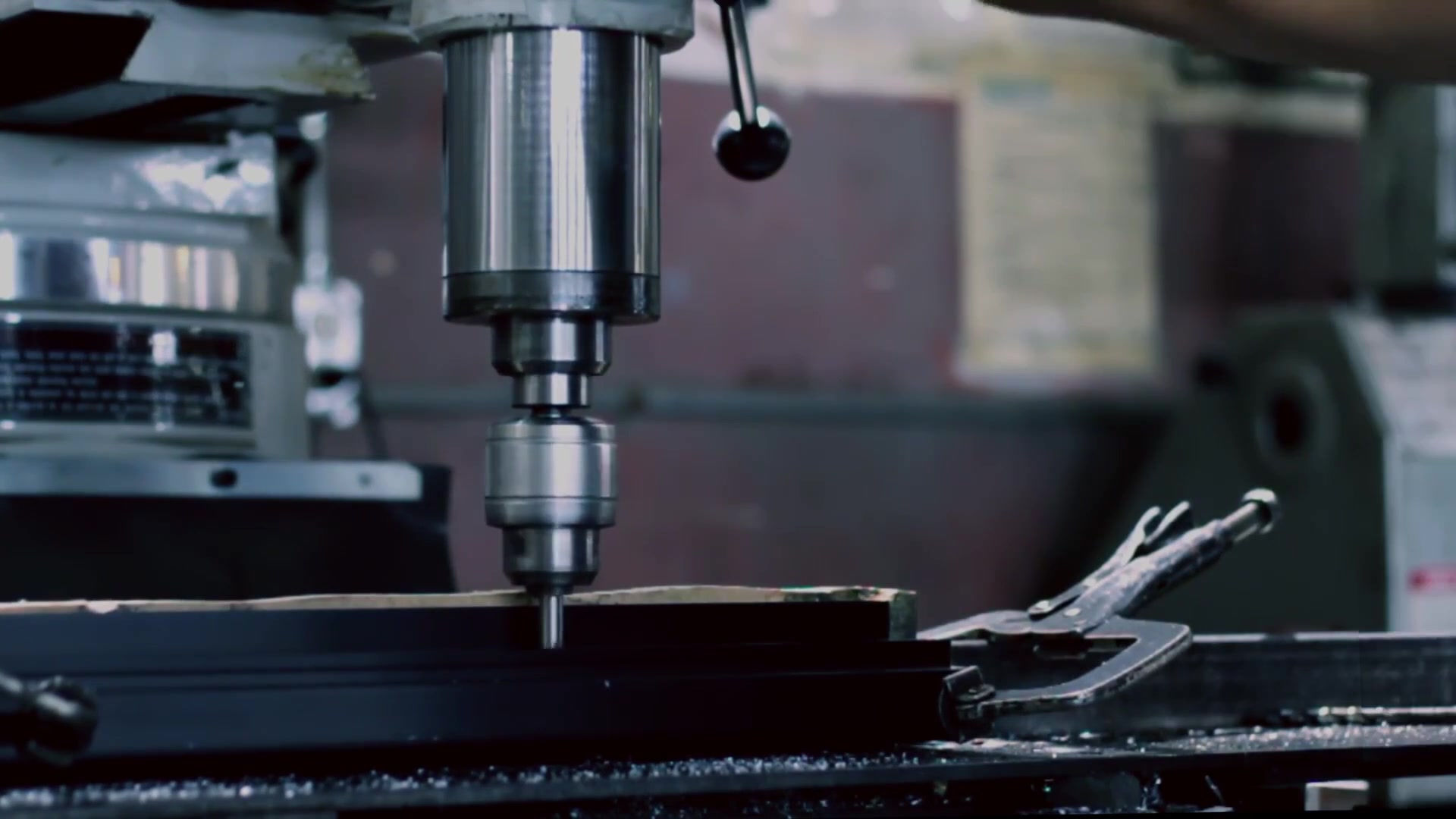
Machined Components & Milling & Turning, CNC Machined Parts, Custom Drill Bits, Shaft Machining at AGS-TECH Machined Components & Milling & Turning CNC machined part manufactured and assembled by AGS-TECH Inc. CNC machined parts for food packaging industry www.agstech.net CNC machined parts High volume CNC turning, milling and drilling Custom drill bits manufactured for a client High quality CNC machining and finishing Threading - Thread Rolling and Cutting by AGS-TECH Inc. Precision Machining offered by AGS-TECH Inc. CNC manufacturing by AGS-TECH Inc. CNC Spring Forming by AGS-TECH Inc. EDM Machining of Rotor AGS-TECH Inc. EDM Machined Steel Part AGS-TECH Inc. Thread Forming by AGS-TECH Inc. Cannulated drill bits machining by AGS-TECH Inc. Machined shaft of a stirrer Stainless Steel Forming Shaping Cutting Grinding Polishing by AGS-TECH Inc. Machined Tool Parts Manufactured by AGS-TECH Inc. Rapid Prototyping of Metal Components Black anodized aluminum parts Brass parts machining CNC turning of a stainless steel part Manufactured Shafts Precision knurled pneumatic components manufactured by AGS-TECH Inc. Precision machined tiny gear and dials manufactured by AGS-TECH Inc Machining of industrial sapphire Industrial sapphire CNC machining Technical ceramic rings made by AGS-TECH, Inc. Cylinder Head by AGS-TECH Inc. Cylinder Head Pneumatic Hydraulic and Vacuum Components Machining - AGS-TECH Custom Skive Blades Machining and Deburring Hardness testing of Skive Blades Cutting tools manufactured to certain hardness specification. Machined bushings produced inexpensively by AGS-TECH Inc Machined Bushings - AGS-TECH Inc Specialty DU Bearings Precision Machined DU Bearing Machine Elements from Steel Machined Machine Elements with Yellow Zinc Chromate Finish PREVIOUS PAGE
- Optomechanical Assembly, Endoscope Coupler Manufacturing, Optocouplers
Optomechanical Assembly, Endoscope Coupler Manufacturing, Optocouplers Custom Fabrication Optomechanical Assemblies Optomechanical assemblies Optomechanical Assemblies - AGS-TECH Optical Projector Assemblies from AGS-TECH Inc. Optomechanical Assemblies - Camera Systems - AGS-TECH, Inc. AGS-TECH designs and manufactures optocouplers such as Iphone to endoscope coupler Fiberscope supplied by AGS-TECH Inc. Optomechanical Components Mirror Finish Reflective Sheet Metal Assembly for Solar Application by AGS-TECH Inc. PREVIOUS PAGE
- Embedded Systems, Embedded Computer, Industrial Computers, Janz Tec
Embedded Systems, Embedded Computer, Industrial Computers, Janz Tec, Korenix, Industrial Workstations, Servers, Computer Rack, Single Board Computer Embedded Systems & Industrial Computers & Panel PC Read More Embedded Systems & Computers Read More Panel PC, Multitouch Displays, Touch Screens Read More Industrial PC Read More Industrial Workstations Read More Networking Equipment, Network Devices, Intermediate Systems, Interworking Unit Read More Storage Devices, Disk Arrays and Storage Systems, SAN, NAS Read More Industrial Servers Read More Chassis,Racks,Mounts for Industrial Computers Read More Accessories, Modules, Carrier Boards for Industrial Computers Read More Automation & Intelligent Systems Being an industrial products supplier we offer you some of the most indispensable industrial computers & servers & networking & storage devices, embedded computer and systems, single board computers, panel PC, industrial PC, rugged computer, touch screen computers, industrial workstation, industrial computer components & accessories, digital and analog I/O devices, routers, bridge, switching equipment, hub, repeater, proxy, firewall, modem, network interface controller, protocol converter, network attached storage (NAS) arrays, storage area network (SAN) arrays, multichannel relay modules, Full-CAN controller for MODULbus sockets, MODULbus carrier board, incremental encoder module, intelligent PLC link concept, motor controller for DC servo motors, serial interface module, VMEbus prototyping board, intelligent profibus DP slave interface, software, related electronics, chassis-racks-mounts. We bring the best of the World's industrial computer products from factory to your door. Our advantage is in being able to offer you different brand names such as Janz Tec and Korenixfor list prices or lower from our stores. Also what makes us special is our ability to offer you variations of products / custom configurations / integration with other systems that you cannot procure from other sources. We offer you brand name high quality equipment for the list price or lower. There are significant discounts to the posted prices if your quantity of order is significant. Most of our equipment is in stock. If not in stock, since we are a preferred reseller and distributor we can still supply it within a shorter lead time to you. In addition to stock items we are capable to offer you special products designed and manufactured according to your needs. Just let us know what differences you need on your industrial computer system and we will get it made according to your needs and requests. We offer you CUSTOM MANUFACTURING and ENGINEERING INTEGRATION capability. We also build CUSTOM AUTOMATION SYSTEMS, MONITORING and PROCESS CONTROL SYSTEMS by integrating computers, translation stages, rotary stages, motorized components, arms, data acquisition cards, process control cards, sensors, actuators and other hardware and software components of need. Regardless of your location on earth, we ship within a few days to your door. We have discounted shipment agreements with UPS, FEDEX, TNT, DHL and standard air. You can order online using options such as credit cards using our PayPal account, wire transfer, certified check or money order. If you would like to speak to us before making a decision or if you have any questions, all you need is to call us and one of our seasoned computer and automation engineers will help you. To be closer to you, we have offices and warehouses at various global locations. Click on the relevant submenus above to read more about our products in the category of industrial computer. Dowload brochure for our DESIGN PARTNERSHIP PROGRAM For more detailed information, we also invite you to visit our industrial computer store http://www.agsindustrialcomputers.com CLICK Product Finder-Locator Service PREVIOUS PAGE
- Cutting Drilling Grinding Polishing Dicing Tools , USA , AGS-TECH Inc.
We offer a large variety of cutting tools, drilling tools, grinding tool, polishing tools, lapping, dicing tool, material shaping tools, blades, drill bits, and more Cutting, Drilling, Grinding, Lapping, Polishing, Dicing and Shaping Tools We have a wide selection of cutting, grinding, lapping, polishing, dicing and shaping tools that can be used in machine shops, auto mechanics, by carpenter's, construction sites, equipment manufacturers....etc. Our cutting, drilling, grinding, lapping, polishing, dicing and shaping tools, blades, discs, drill bits... are manufactured at ISO9001 or TS16949 certified plants and conform to internationally accepted industry standards. Please click on the highlighted text below to move to the relevant submenu: Hole Saws Metal Cutting & Shaping Tools Wood Cutting Shaping Tools Masonry Cutting Shaping Tools Cutting & Grinding Disc Diamond Tools Glass Cutting Shaping Tools Gear Cutting Shaping Tools Specialty Cutting Tools Equipment to Cut Drill Polish Read More Read More Read More Read More Read More Read More Read More Read More Read More Read More CLICK Product Finder-Locator Service PREVIOUS PAGE
- Thermal Infrared Test Equipment, Thermal Camera, Differential Scanning
Thermal Infrared Test Equipment, Thermal Camera, Differential Scanning Calorimeter, Thermo Gravimetric Analyzer, Thermo Mechanical Analyzer, Dynamic Mechanical Thermal & IR Test Equipment CLICK Product Finder-Locator Service Among the many THERMAL ANALYSIS EQUIPMENT, we focus our attention to the popular ones in industry, namely the DIFFERENTIAL SCANNING CALORIMETRY ( DSC ), THERMO-GRAVIMETRIC ANALYSIS ( TGA ), THERMO-MECHANICAL ANALYSIS ( TMA ), DILATOMETRY,DYNAMIC MECHANICAL ANALYSIS ( DMA ), DIFFERENTIAL THERMAL ANALYSIS ( DTA). Our INFRARED TEST EQUIPMENT involves THERMAL IMAGING INSTRUMENTS, INFRARED THERMOGRAPHERS, INFRARED CAMERAS. Some applications for our thermal imaging instruments are Electrical and Mechanical System Inspection, Electronic Component Inspection, Corrosion Damage and Metal Thinning, Flaw Detection. Please download catalogs from colored links below and let us know your prefered brand and model number of the product. You can purchase brand new or refurbished / used Thermal & IR Test Equipment from us: FLUKE Test Tools Catalog (includes Thermal Imagers, Thermometers) HAIDA Color Assessment Cabinet Private Label Hand Tools for Every Industry (This catalog contains a few thermal & IR test instruments. We can private label these hand tools if you wish. In other words, we can put your company name, brand and label on them. This way you can promote your brand by reselling these to your customers.) DIFFERENTIAL SCANNING CALORIMETERS (DSC) : A technique in which the difference in the amount of heat required to increase the temperature of a sample and reference is measured as a function of temperature. Both the sample and reference are maintained at nearly the same temperature throughout the experiment. The temperature program for a DSC analysis is established so that the sample holder temperature increases linearly as a function of time. The reference sample has a well-defined heat capacity over the range of temperatures to be scanned. DSC experiments provide as a result a curve of heat flux versus temperature or versus time. Differential scanning calorimeters are frequently used to study what happens to polymers when they're heated. The thermal transitions of a polymer can be studied using this technique. Thermal transitions are changes that take place in a polymer when they are heated. The melting of a crystalline polymer is an example. The glass transition is also a thermal transition. DSC thermal analysis is carried out for determining Thermal Phase Changes, Thermal Glass Transition Temperature (Tg), Crystalline Melt Temperatures, Endothermic Effects, Exothermic Effects, Thermal Stabilities, Thermal Formulation Stabilities, Oxidative Stabilities, Transition Phenomena, Solid State Structures. DSC analysis determines the Tg Glass Transition Temperature, temperature at which amorphous polymers or an amorphous part of a crystalline polymer go from a hard brittle state to a soft rubbery state, melting point, temperature at which a crystalline polymer melts, Hm Energy Absorbed (joules/gram), amount of energy a sample absorbs when melting, Tc Crystallization Point, temperature at which a polymer crystallizes upon heating or cooling, Hc Energy Released (joules/gram), amount of energy a sample releases when crystallizing. Differential Scanning Calorimeters can be used to determine the thermal properties of plastics, adhesives, sealants, metal alloys, pharmaceutical materials, waxes, foods, oils and lubricants and catalysts….etc. DIFFERENTIAL THERMAL ANALYZERS (DTA): An alternative technique to DSC. In this technique it is the heat flow to the sample and reference that remains the same instead of the temperature. When the sample and reference are heated identically, phase changes and other thermal processes cause a difference in temperature between the sample and reference. DSC measures the energy required to keep both the reference and the sample at the same temperature whereas DTA measures the difference in temperature between the sample and the reference when they are both put under the same heat. So they are similar techniques. THERMOMECHANICAL ANALYZER (TMA) : The TMA reveals the change in the dimensions of a sample as a function of temperature. One can regard TMA as a very sensitive micrometer. The TMA is a device that allows precise measurements of position and can be calibrated against known standards. A temperature control system consisting of a furnace, heat sink and a thermocouple surrounds the samples. Quartz, invar or ceramic fixtures hold the samples during tests. TMA measurements record changes caused by changes in the free volume of a polymer. Changes in free volume are volumetric changes in the polymer caused by the absorption or release of heat associated with that change; the loss of stiffness; increased flow; or by the change in relaxation time. The free volume of a polymer is known to be related to viscoelasticity, aging, penetration by solvents, and impact properties. The glass transition temperature Tg in a polymer corresponds to the expansion of the free volume allowing greater chain mobility above this transition. Seen as an inflection or bending in the thermal expansion curve, this change in the TMA can be seen to cover a range of temperatures. The glass transition temperature Tg is calculated by an agreed upon method. Perfect agreement is not immediately witnessed in the value of the Tg when comparing different methods, however if we carefully examine the agreed upon methods in determining the Tg values then we understand that there is actually good agreement. Besides its absolute value, the width of the Tg is also an indicator of changes in the material. TMA is a relatively simple technique to carry out. TMA is often used for measuring Tg of materials such as highly cross-linked thermoset polymers for which the Differential Scanning Calorimeter (DSC) is difficult to use. In addition to Tg, the coefficient of thermal expansion (CTE) is obtained from thermomechanical analysis. The CTE is calculated from the linear sections of the TMA curves. Another useful result the TMA can provide us is finding out the orientation of crystals or fibers. Composite materials may have three distinct thermal expansion coefficients in the x, y and z directions. By recording the CTE in x, y and z directions one may understand in which direction fibers or crystals are predominantly oriented. To measure the bulk expansion of the material a technique called DILATOMETRY can be used. The sample is immersed in a fluid such as silicon oil or Al2O3 powder in the dilatometer, run thru the temperature cycle and the expansions in all directions are converted to a vertical movement, which is measured by the TMA. Modern thermomechanical analyzers make this easy for users. If a pure liquid is used, the dilatometer is filled with that liquid instead of the silicon oil or alumina oxide. Using diamond TMA the users can run stress strain curves, stress relaxation experiments, creep-recovery and dynamic mechanical temperature scans. The TMA is an indispensible test equipment for industry and research. THERMOGRAVIMETRIC ANALYZERS ( TGA ) : Thermogravimetric Analysis is a technique where the mass of a substance or specimen is monitored as a function of temperature or time. The sample specimen is subjected to a controlled temperature program in a controlled atmosphere. The TGA measures a sample’s weight as it is heated or cooled in its furnace. A TGA instrument consists of a sample pan that is supported by a precision balance. That pan resides in a furnace and is heated or cooled during the test. The mass of the sample is monitored during the test. Sample environment is purged with an inert or a reactive gas. Thermogravimetric analyzers can quantify loss of water, solvent, plasticizer, decarboxylation, pyrolysis, oxidation, decomposition, weight % filler material, and weight % ash. Depending on the case, information may be obtained upon heating or cooling. A typical TGA thermal curve is displayed from left to right. If the TGA thermal curve descends, it indicates a weight loss. Modern TGAs are capable of conducting isothermal experiments. Sometimes the user may want to use a reactive sample purge gases, such as oxygen. When using oxygen as a purge gas user may want to switch gases from nitrogen to oxygen during the experiment. This technique is frequently used to identify the percent carbon in a material. Thermogravimetric analyzer can be used to compare two similar products, as a quality control tool to ensure products meet their material specifications, to ensure products meet safety standards, to determine carbon content, identifying counterfeit products, to identify safe operating temperatures in various gases, to enhance product formulation processes, to reverse engineer a product. Finally it is worth mentioning that combinations of a TGA with a GC/MS are available. GC is short for Gas Chromatography and MS is short for Mass Spectrometry. DYNAMIC MECHANICAL ANALYZER ( DMA) : This is a technique where a small sinusoidal deformation is applied to a sample of known geometry in a cyclic manner. The materials response to stress, temperature, frequency and other values is then studied. The sample can be subjected to a controlled stress or a controlled strain. For a known stress, the sample will deform a certain amount, depending on its stiffness. DMA measures stiffness and damping, these are reported as modulus and tan delta. Because we are applying a sinusoidal force, we can express the modulus as an in-phase component (the storage modulus), and an out of phase component (the loss modulus). The storage modulus, either E’ or G’, is the measure of the sample’s elastic behavior. The ratio of the loss to the storage is the tan delta and is called damping. It is considered a measure of the energy dissipation of a material. Damping varies with the state of the material, its temperature, and with the frequency. DMA is sometimes called DMTA standing for DYNAMIC MECHANICAL THERMAL ANALYZER. Thermomechanical Analysis applies a constant static force to a material and records the material dimensional changes as temperature or time varies. The DMA on the other hand, applies an oscillatory force at a set frequency to the sample and reports changes in stiffness and damping. DMA data provides us modulus information whereas the TMA data gives us the coefficient of thermal expansion. Both techniques detect transitions, but DMA is much more sensitive. Modulus values change with temperature and transitions in materials can be seen as changes in the E’ or tan delta curves. This includes glass transition, melting and other transitions that occur in the glassy or rubbery plateau which are indicators of subtle changes in the material. THERMAL IMAGING INSTRUMENTS, INFRARED THERMOGRAPHERS, INFRARED CAMERAS : These are devices that form an image using infrared radiation. Standard everyday cameras form images using visible light in the 450–750 nanometer wavelength range. Infrared cameras however operate in the infrared wavelength range as long as 14,000 nm. Generally, the higher an object's temperature, the more infrared radiation is emitted as black-body radiation. Infrared cameras work even in total darkness. Images from most infrared cameras have a single color channel because the cameras generally use an image sensor that does not distinguish different wavelengths of infrared radiation. To differentiate wavelengths color image sensors require a complex construction. In some test instruments these monochromatic images are displayed in pseudo-color, where changes in color are used rather than changes in intensity to display changes in the signal. The brightest (warmest) parts of images are customarily colored white, intermediate temperatures are colored red and yellow, and the dimmest (coolest) parts are colored black. A scale is generally shown next to a false color image to relate colors to temperatures. Thermal cameras have resolutions considerably lower than that of optical cameras, with values in the neighborhood of 160 x 120 or 320 x 240 pixels. More expensive infrared cameras can achieve a resolution of 1280 x 1024 pixels. There are two main categories of thermographic cameras: COOLED INFRARED IMAGE DETECTOR SYSTEMS and UNCOOLED INFRARED IMAGE DETECTOR SYSTEMS. Cooled thermographic cameras have detectors contained in a vacuum-sealed case and are cryogenically cooled. The cooling is necessary for the operation of the semiconductor materials used. Without cooling, these sensors would be flooded by their own radiation. Cooled infrared cameras are however expensive. Cooling requires much energy and is time-consuming, requiring several minutes of cooling time prior to working. Although the cooling apparatus is bulky and expensive, cooled infrared cameras offer users superior image quality compared to uncooled cameras. The better sensitivity of cooled cameras allows the use of lenses with higher focal length. Bottled nitrogen gas can be used for cooling. Uncooled thermal cameras use sensors operating at ambient temperature, or sensors stabilized at a temperature close to ambient using temperature control elements. Uncooled infrared sensors are not cooled to low temperatures and therefore do not require bulky and expensive cryogenic coolers. Their resolution and image quality however is lower as compared to cooled detectors. Thermographic cameras offer many opportunities. Overheating spots is power lines can be located and repaired. Electric circuitry can be observed and unusually hot spots can indicate problems such as short circuit. These cameras are also widely used in buildings and energy systems to locate places where there is significant heat loss so that better heat insulation can be considered at those points. Thermal imaging instruments serve as non-destructive test equipment. For details and other similar equipment, please visit our equipment website: http://www.sourceindustrialsupply.com PREVIOUS PAGE
- Casting and Machined Parts, CNC Manufacturing, Milling, Turning, Swiss
Casting and Machined Parts, CNC Manufacturing, Milling, Turning, Swiss Type Machining, Die Casting, Investment Casting, Lost Foam Cast Parts from AGS-TECH Inc. Casting and Machining Our custom casting and machining techniques are expendable and non-expendable castings, ferrous and nonferrous casting, sand, die, centrifugal, continuous, ceramic mold, investment, lost foam, near-net-shape, permanent mold (gravity die casting), plaster mold (plaster casting) and shell castings, machined parts produced by milling and turning using conventional as well as CNC equipment, swiss type machining for high throughput inexpensive small precision parts, screw machining for fasteners, non-conventional machining. Please keep in mind that besides metals and metal alloys, we machine ceramic, glass and plastic components as well in some cases when manufacturing a mould is not appealing or not the option. Machining of polymer materials requires the specialized experience we have because of the challenge plastics and rubber presents due to their softness, non-rigidity...etc. For machining of ceramic and glass, please see our page on Non-Conventional Fabrication. AGS-TECH Inc. manufactures and supplies both lightweight and heavy castings. We have been supplying metal castings and machined parts for boilers, heat exchangers, automobiles, micromotors, wind turbines, food packaging equipment and more. We recommend that you click here to DOWNLOAD our Schematic Illustrations of Machining and Casting Processes by AGS-TECH Inc. This will help you better understand the information we are providing you below. Let’s look at some of the various techniques we offer in detail: • EXPENDABLE MOLD CASTING : This broad category refers to methods that involve temporary and non-reusable molds. Examples are sand, plaster, shell, investment (also called lost-wax) and plaster casting. • SAND CASTING : A process where sand is used as the mold material. A very old method and still very popular to the extent that the majority of metal castings produced are made by this technique . Low cost even at low quantity production. Suitable for small and large parts manufacturing. The technique can be used to manufacture parts within days or weeks with very little investment. The moist sand is bonded together using clay, binders or special oils. Sand is generally contained in mold boxes and cavity & gate system are created by compacting the sand around models. The processes are: 1.) Placing of the model in sand to make the mold 2.) Incorporation of model and sand in a gating system 3.) Removal of model 4.) Filling of mold cavity with molten metal 5.) Cooling of the metal 6.) Breaking the sand mold and removal of the casting • PLASTER MOLD CASTING : Similar to sand casting, and instead of sand, plaster of paris is being used as the mold material. Short production lead times like sand casting and inexpensive. Good dimensional tolerances and surface finish. Its major disadvantage is that it can only be used with low melting point metals like aluminum and zinc. • SHELL MOLD CASTING : Also similar to sand casting. Mold cavity obtained by hardened shell of sand and thermosetting resin binder instead of flask filled with sand as in sand casting process. Almost any metal suitable to be cast by sand can be cast by shell molding. The process can be summarized as: 1.) Manufacturing of the shell mold. Sand used is of a much smaller grain size when compared to sand used in sand casting. The fine sand is mixed with thermosetting resin. The metal pattern is coated with a parting agent to make removal of the shell easier. Thereafter the metal pattern is heated and the sand mixture is pored or blown onto the hot casting pattern. A thin shell forms on the surface of the pattern. The thickness of this shell can be adjusted by varying the length of time the sand resin mixture is in contact with the metal pattern. The loose sand is then removed with the shell covered pattern remaining. 2.) Next, the shell and pattern are heated in an oven so that the shell hardens. After hardening is complete, the shell is ejected from pattern using pins built into the pattern. 3.) Two such shells are assembled together by gluing or clamping and make up the complete mold. Now the shell mold is inserted into a container in which it is supported by sand or metal shot during the casting process. 4.) Now the hot metal can be poured into the shell mold. Advantages of shell casting are products with very good surface finish, possibility of manufacturing complex parts with high dimensional accuracy, process easy to automate, economical for large volume production. Disadvantages are the molds necessitate good ventilation because of gases that are created when molten metal contacts the binder chemical, the thermosetting resins and metal patterns are expensive. Due to the cost of metal patterns, the technique may not suit well for low quantity production runs. • INVESTMENT CASTING ( also known as LOST-WAX CASTING ): Also a very old technique and suitable for manufacturing quality parts with high accuracy, repeatability, versatility and integrity from many metals, refractory materials and special high performance alloys. Small as well as large sized parts can be produced. An expensive process when compared to some of the other methods, but major advantage is the possibility to produce parts with near net shape, intricate contours and details. So the cost is somewhat offset by the elimination of rework and machining in some cases. Even though there can be variations, here is a summary of the general investment casting process: 1.) Creation of original master pattern from wax or plastic. Each casting needs one pattern as these are destroyed in the process. Mold from which patterns are manufactured is also needed and most of the time the mold is cast or machined. Because the mold does not need to be opened, complex castings can be achieved, many wax patterns can be connected like the branches of a tree and poured together, thus enabling production of multiple parts from a single pouring of the metal or metal alloy. 2.) Next, the pattern is dipped or poured over with a refractory slurry composed of very fine grained silica, water, binders. This results in a ceramic layer over the surface of the pattern. The refractory coat on pattern is left to dry and harden. This step is where the name investment casting comes from: Refractory slurry is invested over the wax pattern. 3.) At this step, the hardened ceramic mould is turned upside down and heated so that the wax melts and pours out of the mould. A cavity is left behind for the metal casting. 4.) After the wax is out, the ceramic mold is heated to even a higher temperature which results in strengthening of the mold. 5.) Metal casting is poured into the hot mold filling all intricate sections. 6.) Casting is allowed to solidify 7.) Finally the ceramic mould is broken and manufactured parts are cut from the tree. Here is a link to Investment Casting Plant Brochure • EVAPORATIVE PATTERN CASTING : The process uses a pattern made from a material such as polystyrene foam that will evaporate when hot molten metal is poured into the mold. There are two types of this process: LOST FOAM CASTING which uses unbonded sand and FULL MOLD CASTING which uses bonded sand. Here are the general process steps: 1.) Manufacture the pattern from a material such as polystyrene. When large quantities will be manufactured, the pattern is molded. If part has a complex shape, several sections of such foam material may need to be adhered together to form the pattern. We often coat the pattern with a refractory compound to create a good surface finish on the casting. 2.) The pattern is then put into molding sand. 3.) The molten metal is poured into the mould, evaporating the foam pattern, i.e. polystyrene in most cases as it flows through the mold cavity. 4.) The molten metal is left in the sand mold to harden. 5.) After it is hardened, we remove the casting. In some cases, the product we manufacture requires a core within the pattern. In evaporative casting, there is no need to place and secure a core in the mold cavity. The technique is suitable for manufacturing of very complex geometries, it can be easily automated for high volume production, and there are no parting lines in the cast part. The basic process is simple and economical to implement. For large volume production, since a die or mold is needed to produce the patterns from polystyrene, this may be somewhat costly. • NON-EXPANDABLE MOLD CASTING : This broad category refers to methods where the mold does not need to be reformed after each production cycle. Examples are permanent, die, continuous and centrifugal casting. Repeatability is obtained and parts can be characterized as NEAR NET SHAPE. • PERMANENT MOLD CASTING : Reusable molds made from metal are used for multiple castings. A permanent mold can generally be used for tens of thousands of times before it wears out. Gravity, gass pressure or vacuum are generally used to fill the mould. Molds (also called die) is generally made of iron, steel, ceramic or other metals. The general process is: 1.) Machine and create the mould. It is common to machine the mold out of two metal blocks that fit together and can be opened and closed. Both the part features as well as the gating system is generally machined into the casting mould. 2.) The internal mold surfaces are coated with a slurry incorporating refractory materials. This helps to control heat flow and acts as a lubricant for easy removal of the cast part. 3.) Next, the permanent mold halves are closed and the mold is heated. 4.) Molten metal is poured into mould and let still for solidification. 5.) Before much cooling occurs, we remove the part from permanent mold using ejectors when mold halves are opened. We frequently use permanent mold casting for low melting point metals such as zinc and aluminum. For steel castings, we use graphite as mold material. We sometimes obtain complex geometries using cores within permanent molds. Advantages of this technique are castings with good mechanical properties obtained by rapid cooling, uniformity in properties, good accuracy and surface finish, low reject rates, possibility of automating the process and producing high volumes economically. Disadvantages are high initial setup costs which make it unsuitable for low volume operations, and limitations on the size of the parts manufactured. • DIE CASTING : A die is machined and molten metal is pushed under high pressure into mold cavities. Both nonferrous as well as ferrous metal die castings are possible. The process is suitable for high quantity production runs of small to medium sized parts with details, extremely thin walls, dimensional consistency and good surface finish. AGS-TECH Inc. is capable to manufacture wall thicknesses as small as 0.5 mm using this technique. Like in permanent mold casting, the mold needs to consist of two halves that can open and close for removal of part produced. A die casting mold may have multiple cavities to enable production of multiple castings with each cycle. Die casting molds are very heavy and much larger than the parts they produce, therefore also expensive. We repair and replace worn out dies free of charge for our customers as long as they reorder their parts from us. Our dies have long lifetimes in the several hundred thousand cycles range. Here are the basic simplified process steps: 1.) Production of the mold generally from steel 2.) Mold installed on die casting machine 3.) The piston forces molten metal to flow in the die cavities filling out the intricate features and thin walls 4.) After filling the mold with the molten metal, the casting is let hardened under pressure 5.) Mold is opened and casting removed with the help of ejector pins. 6.) Now the empty die are lubricated again and are clamped for the next cycle. In die casting, we frequently use insert molding where we incorporate an additional part into the mold and cast the metal around it. After solidification, these parts become part of the cast product. Advantages of die casting are good mechanical properties of the parts, possibility of intricate features, fine details and good surface finish, high production rates, easy automation. Disadvantages are: Not very suitable for low volume because of high die and equipment cost, limitations in shapes that can be cast, small round marks on cast parts resulting from contact of ejector pins, thin flash of metal squeezed out at the parting line, need for vents along the parting line between the die, necessity to keep mold temperatures low using water circulation. • CENTRIFUGAL CASTING : Molten metal is poured into the center of the rotating mold at the axis of rotation. Centrifugal forces throw the metal towards the periphery and it is let to solidify as the mold keeps rotating. Both horizontal and vertical axis rotations can be used. Parts with round inner surfaces as well as other non-round shapes can be cast. The process can be summarized as: 1.) Molten metal is poured into centrifugal mould. The metal is then forced to the outer walls due to spinning of the mold. 2.) As the mold rotates, the metal casting hardens Centrifugal casting is a suitable technique for production of hollow cylindirical parts like pipes, no need for sprues, risers and gating elements, good surface finish and detailed features, no shrinkage issues, possibility to produce long pipes with very large diameters, high rate production capability. • CONTINUOUS CASTING ( STRAND CASTING ) : Used to cast a continuous length of metal. Basically the molten metal is cast into two dimensional profile of the mold but its length is indeterminate. New molten metal is constantly fed into the mould as the casting travels downward with its length increasing with time. Metals such as copper, steel, aluminum are cast into long strands using continuous casting process. The process may have various configurations but the common one can be simplified as: 1.) Molten metal is poured into a container located high above the mold at well calculated amounts and flow rates and flows through the water cooled mold. The metal casting poured into the mould solidifies to a starter bar placed at the bottom of the mold. This starter bar gives the rollers something to grab onto initially. 2.) The long metal strand is carried by rollers at a constant speed. The rollers also change the direction of the flow of metal strand from vertical to horizontal. 3.) After the continuous casting has travelled a certain horizontal distance, a torch or saw that moves with the casting quickly cuts it to desired lengths. Continuous casting process can be integrated with ROLLING PROCESS, where the continuously cast metal can be fed directly into a rolling mill to produce I-Beams, T-Beams….etc. Continuous casting produces uniform properties throughout the product, it has a high solidification rate, reduces cost due to very low loss of material, offers a process where loading of metal, pouring, solidification, cutting and casting removal all take place in a continuous operation and thus resulting in high productivity rate and high quality. A major consideration is however the high initial investment, setup costs and space requirements. • MACHINING SERVICES : We offer three, four and five - axis machining. The type of machining processes we use are TURNING, MILLING, DRILLING, BORING, BROACHING, PLANING, SAWING, GRINDING, LAPPING, POLISHING and NON-TRADITIONAL MACHINING which is further elaborated under a different menu of our website. For most of our manufacturing, we use CNC machines. However for some operations conventional techniques are a better fit and therefore we rely on them as well. Our machining capabilities reach the highest level possible and some most demanding parts are manufactured at an AS9100 certified plant. Jet engine blades require highly specialized manufacturing experience and the right equipment. Aerospace industry has very strict standards. Some components with complex geometrical structures are most easily manufactured by five axis machining, which is found only in some machining plants including ours. Our aerospace certified plant has the necessary experience complying to extensive documentation requirement of the aerospace industry. In TURNING operations, a workpiece is rotated and moved against a cutting tool. For this process a machine called lathe is being used. In MILLING, a machine called milling machine has a rotating tool to bring cutting edges to bear against a workpiece. DRILLING operations involve a rotating cutter with cutting edges that produces holes upon contact with the workpiece. Drill presses, lathes or mills are generally used. In BORING operations a tool with a single bent pointed tip is moved into a rough hole in a spinning workpiece to slightly enlarge the hole and improve accuracy. It is used for fine finishing purposes. BROACHING involves a toothed tool to remove material from a workpiece in one pass of the broach (toothed tool). In linear broaching, the broach runs linearly against a surface of the workpiece to effect the cut, whereas in rotary broaching, the broach is rotated and pressed into the workpiece to cut an axis symmetric shape. SWISS TYPE MACHINING is one of our valuable techniques we use for high volume manufacturing of small high precision parts. Using Swiss-type lathe we turn small, complex, precision parts inexpensively. Unlike conventional lathes where the workpiece is kept stationary and tool moving, in Swiss-type turning centers, the workpiece is allowed to move in the Z-axis and the tool is stationary. In Swiss-type machining, the bar stock is held in the machine and advanced through a guide bushing in the z-axis, only exposing the portion to be machined. This way a tight grip is ensured and accuracy is very high. Availability of live tools provide the opportunity to mill and drill as the material advances from the guide bushing. The Y-axis of the Swiss-type equipment provides full milling capabilities and saves great amount of time in manufacturing. Furthermore, our machines have drills and boring tools that operate on the part when it is held in the sub spindle. Our Swiss-Type machining capability gives us a fully automated complete machining opportunity in a single operation. Machining is one of the largest segments of AGS-TECH Inc. business. We either use it as a primary operation or a secondary operation after casting or extruding a part so that all drawing specifications are met. • SURFACE FINISHING SERVICES : We offer a vast variety of surface treatments and surface finishing such as surface conditioning to enhance adhesion, depositing thin oxide layer to enhance adhesion of coating, sand blasting, chem-film, anodizing, nitriding, powder coating, spray coating, various advanced metallization and coating techniques including sputtering, electron beam, evaporation, plating, hard coatings such as diamond like carbon (DLC) or titanium coating for drilling and cutting tools. • PRODUCT MARKING & LABELING SERVICES : Many of our customers require marking and labeling, laser marking, engraving on metal parts. If you have any such need, let us discuss which option will be the best for you. Here are some of commonly used metal cast products. Since these are off-the-shelf, you can save on mould costs in case any of these fits your requirements: CLICK HERE TO DOWNLOAD our 11 Series Die-cast Aluminium Boxes from AGS-Electronics CLICK Product Finder-Locator Service PREVIOUS PAGE
