

Global Custom Manufacturer, Integrator, Consolidator, Outsourcing Partner for a Wide Variety of Products & Services.
We are your one-stop source for manufacturing, fabrication, engineering, consolidation, integration, outsourcing of custom manufactured and off-shelf products & services. We also private label / white label your products with your brand name if you wish.
Choose your Language
-
Custom Manufacturing of Parts, Components, Assemblies, Finished Products, Machines and Industrial Equipment
-
Domestic & Global Contract Manufacturing
-
Manufacturing Outsourcing
-
Domestic, Global Procurement of Industrial Products
-
Private labeling / White Labeling your Products with your Brand Name
-
Product Finding & Locating Services
-
Global Design and Channel Partnership
-
Engineering Integration
-
Engineering Services
-
Global Consolidation, Warehousing, Logistics

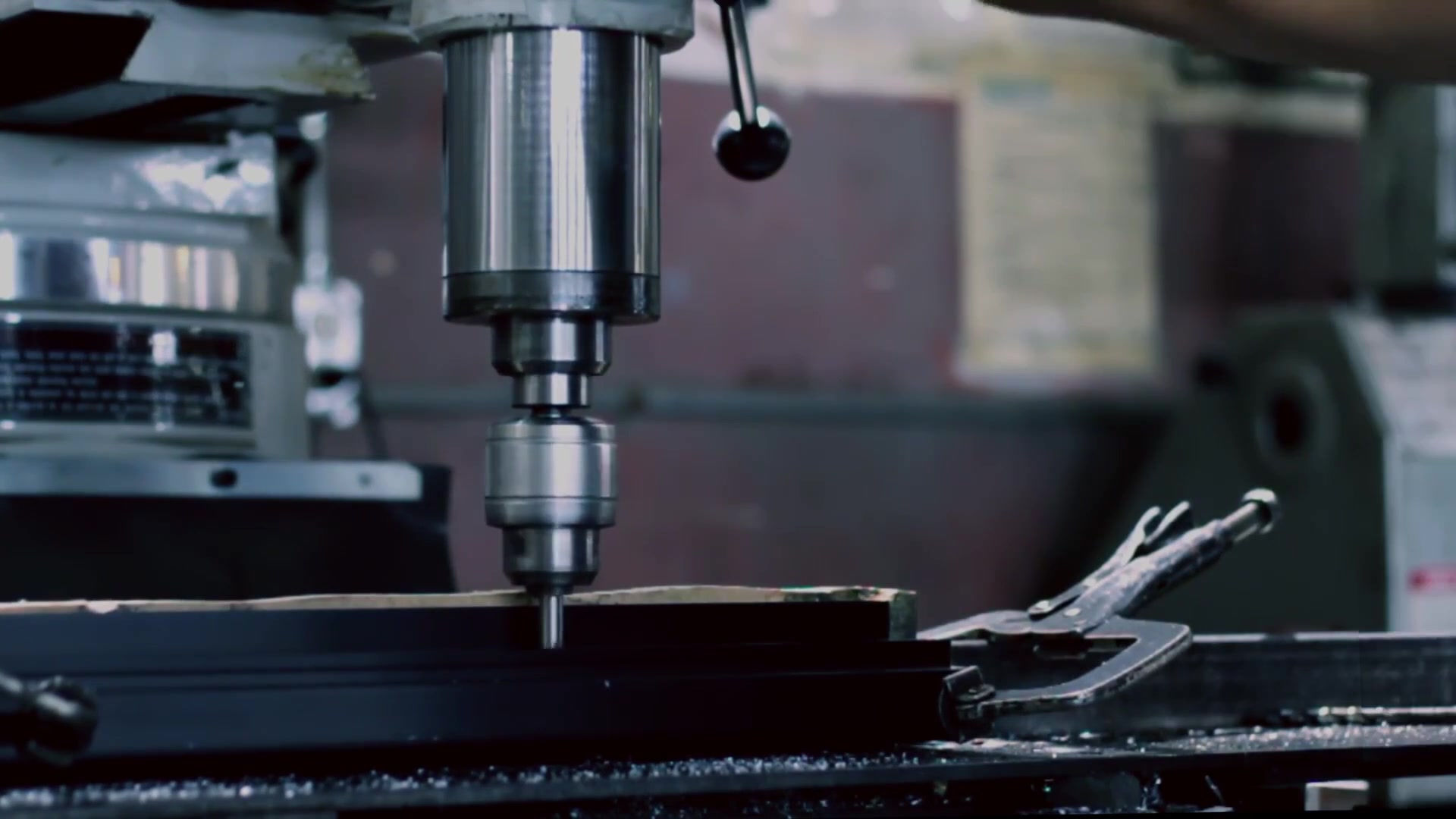
CHEMICAL MACHINING (CM) technique is based on the fact that some chemicals attack metals and etch them. This results in removal of small layers of material from surfaces. We use reagents and etchants such as acids and alkaline solutions to remove material from surfaces. The hardness of the material is not a factor for etching. AGS-TECH Inc. frequently uses chemical machining for engraving metals, manufacturing printed-circuit boards and deburring of produced parts. Chemical machining is well suited for shallow removal up to 12 mm on large flat or curved surfaces, and CHEMICAL BLANKING of thin sheets. The chemical machining (CM) method involves low tooling and equipment costs and is advantageous over other ADVANCED MACHINING PROCESSES for low production runs. Typical material removal rates or cutting speeds in chemical machining are around 0.025 – 0.1 mm/min.
Using CHEMICAL MILLING, we produce shallow cavities on sheets, plates, forgings and extrusions, either to meet design requirements or for reduction of weight in parts. The chemical milling technique can be used on a variety of metals. In our manufacturing processes, we deploy removable layers of maskants to control the selective attack by the chemical reagent on different areas of the workpiece surfaces. In microelectronic industry the chemical milling is widely used to fabricate miniature devices on chips and the technique is referred to as WET ETCHING. Some surface damage may result from chemical milling due to preferential etching and intergranular attack by the chemicals involved. This may result in deterioration of surfaces and roughening. One has to be careful prior to deciding to use chemical milling on metal castings, welded and brazed structures because uneven material removal may occur because the filler metal or the structural material may machine preferentially. In metal castings uneven surfaces may be obtained due to porosity and non-uniformity of the structure.
CHEMICAL BLANKING: We use this method to produce features that penetrate through the thickness of the material, having the material removed by chemical dissolution. This method is an alternative to stamping technique we use in sheet metal manufacturing. Also in burr-free etching of printed-circuit boards (PCB) we deploy chemical blanking.
PHOTOCHEMICAL BLANKING & PHOTOCHEMICAL MACHINING (PCM): Photochemical blanking is also known as PHOTOETCHING or PHOTO ETCHING, and is a modified version of chemical milling. Material is removed from flat thin sheets using photographic techniques and complex burr-free, stress-free shapes are blanked. Using photochemical blanking we manufacture fine and thin metal screens, printed-circuit cards, electric-motor laminations, flat precision springs. The photochemical blanking technique offers us the advantage of producing small parts, fragile parts without the need to manufacture difficult and expensive blanking dies that are used in traditional sheet metal manufacturing. Photochemical blanking does require skilled personnel, but the tooling costs are low, the process is easily automated and feasibility is high for medium to high volume production. Some disadvantages exist as is the case in every manufacturing process: Environmental concerns due to chemicals and safety concerns due to volatile liquids being used.
Photochemical machining also known as PHOTOCHEMICAL MILLING, is the process of fabricating sheet metal components using a photoresist and etchants to corrosively machine away selected areas. Using photo etching we produce highly complex parts with fine details economically. The photochemical milling process is for us an economical alternative to stamping, punching, laser and water jet cutting for thin gauge precision parts. The photochemical milling process is useful for prototyping and allows for easy and quick changes when there is a change in design. It is an ideal technique for research & development. Phototooling is fast and inexpensive to produce. Most phototools cost less than $ 500 and can be produced within two days. Dimensional tolerances are well met with no burrs, no stress and sharp edges. We can start manufacturing a part within hours after receiving your drawing. We can use PCM on most commercially available metals and alloys such as include aluminium, brass, beryllium-copper, copper, molybdenum, inconel, manganese, nickel, silver, steel, stainless steel, zinc and titanium with thicknesses of 0.0005 to 0.080 in (0.013 to 2.0 mm). Phototools are exposed only to light and therefore do not wear out. Due to the cost of hard tooling for stamping and fine blanking, significant volume is required to justify the expense, which is not the case in PCM. We start the PCM process by printing the shape of the part onto optically clear and dimensionally stable photographic film. The phototool consists of two sheets of this film showing negative images of the parts meaning that the area that will become the parts is clear and all of the areas to be etched are black. We register the two sheets optically and mechanically to form the top and bottom halves of the tool. We cut the metal sheets to size, clean and then laminate on both sides with a UV-sensitive photoresist. We place the coated metal between the two sheets of the phototool and a vacuum is drawn to ensure intimate contact between the phototools and the metal plate. We then expose the plate to UV light that allows the areas of resist that are in the clear sections of the film to be hardened. After exposure we wash away the unexposed resist of the plate, leaving the areas to be etched unprotected. Our etching lines have driven-wheel conveyors to move the plates and arrays of spray nozzles above and below the plates. The etchant is typically an aqueous solution of acid such as ferric chloride, that is heated and directed under pressure to both sides of the plate. The etchant reacts with the unprotected metal and corrodes it away. After neutralizing and rinsing, we remove the remaining resist and the sheet of parts is cleaned and dried. Applications of photochemical machining include fine screens and meshes, apertures, masks, battery grids, sensors, springs, pressure membranes, flexible heating elements, RF and microwave circuits and components, semiconductor leadframes, motor and transformer laminations, metal gaskets and seals, shields and retainers, electrical contacts, EMI/RFI shields, washers. Some parts, such as semiconductor leadframes, are very complex and fragile that, despite volumes in the millions of pieces, they can only be produced by photo etching. The accuracy achievable with the chemical etching process offers us tolerances starting at +/-0.010mm depending on the material type and thickness. Features can be positioned with accuracies around +-5 microns. In PCM, the most economical way is to plan the largest sheet size possible consistent with the size and dimensional tolerances of the part. The more parts per sheet are produced the lower the unit labor cost per part. Material thickness affects costs and is proportional to the length of time to etch through. Most alloys etch at rates between 0.0005–0.001 in (0.013–0.025 mm) of depth per minute per side. In general, for steel, copper or aluminum workpieces with thicknesses up to 0.020 in (0.51 mm), part costs will be roughly $0.15–0.20 per square inch. As the geometry of the part becomes more complex, photochemical machining gains greater economic advantage over sequential processes such as CNC punching, laser or water-jet cutting, and electrical discharge machining.
Contact us today with your project and let us provide you our ideas and suggestions.