

Global Custom Manufacturer, Integrator, Consolidator, Outsourcing Partner for a Wide Variety of Products & Services.
We are your one-stop source for manufacturing, fabrication, engineering, consolidation, integration, outsourcing of custom manufactured and off-shelf products & services. We also private label / white label your products with your brand name if you wish.
Choose your Language
-
Custom Manufacturing of Parts, Components, Assemblies, Finished Products, Machines and Industrial Equipment
-
Domestic & Global Contract Manufacturing
-
Manufacturing Outsourcing
-
Domestic, Global Procurement of Industrial Products
-
Private labeling / White Labeling your Products with your Brand Name
-
Product Finding & Locating Services
-
Global Design and Channel Partnership
-
Engineering Integration
-
Engineering Services
-
Global Consolidation, Warehousing, Logistics
Nanoscale & Microscale & Mesoscale Manufacturing

Our NANOMANUFACTURING, MICROMANUFACTURING and MESOMANUFACTURING processes can be categorized as:
Surface Treatments and Modification
Functional Coatings / Decorative Coatings /
Thin Film / Thick Film
Nanoscale Manufacturing / Nanomanufacturing
Microscale Manufacturing / Micromanufacturing
/ Micromachining
Mesoscale Manufacturing / Mesomanufacturing
Microelectronics & Semiconductor Manufacturing
and Fabrication
Microfluidic Devices Manufacturing
Micro-Optics Manufacturing
Micro Assembly and Packaging
Soft Lithography
In every smart product designed today, one can consider an element that will increase efficiency, versatility, reduce power consumption, reduce waste, increase lifetime of the product and thus be environmentally friendly. For this purpose, AGS-TECH is focusing on a number of processes and products that can be incorporated into devices and equipment to achieve these goals.
For example low-friction FUNCTIONAL COATINGS can reduce power consumption. Some other functional coating examples are scratch resistant coatings, anti-wetting SURFACE TREATMENTS and coatings (hydrophobic), wetness promoting (hydrophilic) surface treatment and coatings, anti-fungal coatings, diamond like carbon coatings for cutting and scribing tools, THIN FILMelectronic coatings, thin film magnetic coatings, multilayer optical coatings.
In NANOMANUFACTURING or NANOSCALE MANUFACTURING, we produce parts at nanometer length scales. In practice it refers to manufacturing operations below micrometer scale. Nanomanufacturing is still in its infancy when compared to micromanufacturing, however the trend is in that direction and nanomanufacturing is definitely very important for the near future. Some applications of nanomanufacturing today are carbon nanotubes as reinforcing fibers for composite materials in bicycle frames, baseball bats and tennis racquets. Carbon nanotubes, depending on the orientation of the graphite in the nanotube, can act as semiconductors or conductors. Carbon nanotubes have very high current-carrying capability, 1000 times higher than silver or copper. Another application of nanomanufacturing is nanophase ceramics. By using nanoparticles in producing ceramic materials, we can simultaneously increase both the strength and ductility of the ceramic. Please click on the submenu for more information.
MICROSCALE MANUFACTURING or MICROMANUFACTURING refers to our manufacturing and fabrication processes on a microscopic scale not visible to the naked eye. The terms micromanufacturing, microelectronics, microelectromechanical systems are not limited to such small length scales, but instead, suggest a material and manufacturing strategy. In our micromanufacturing operations some popular techniques we use are lithography, wet and dry etching, thin film coating. A wide variety of sensors & actuators, probes, magnetic hard-drive heads, microelectronic chips, MEMS devices such as accelerometers and pressure sensors among others are manufactured using such micromanufacturing methods. You will find more detailed information on these in the submenus.
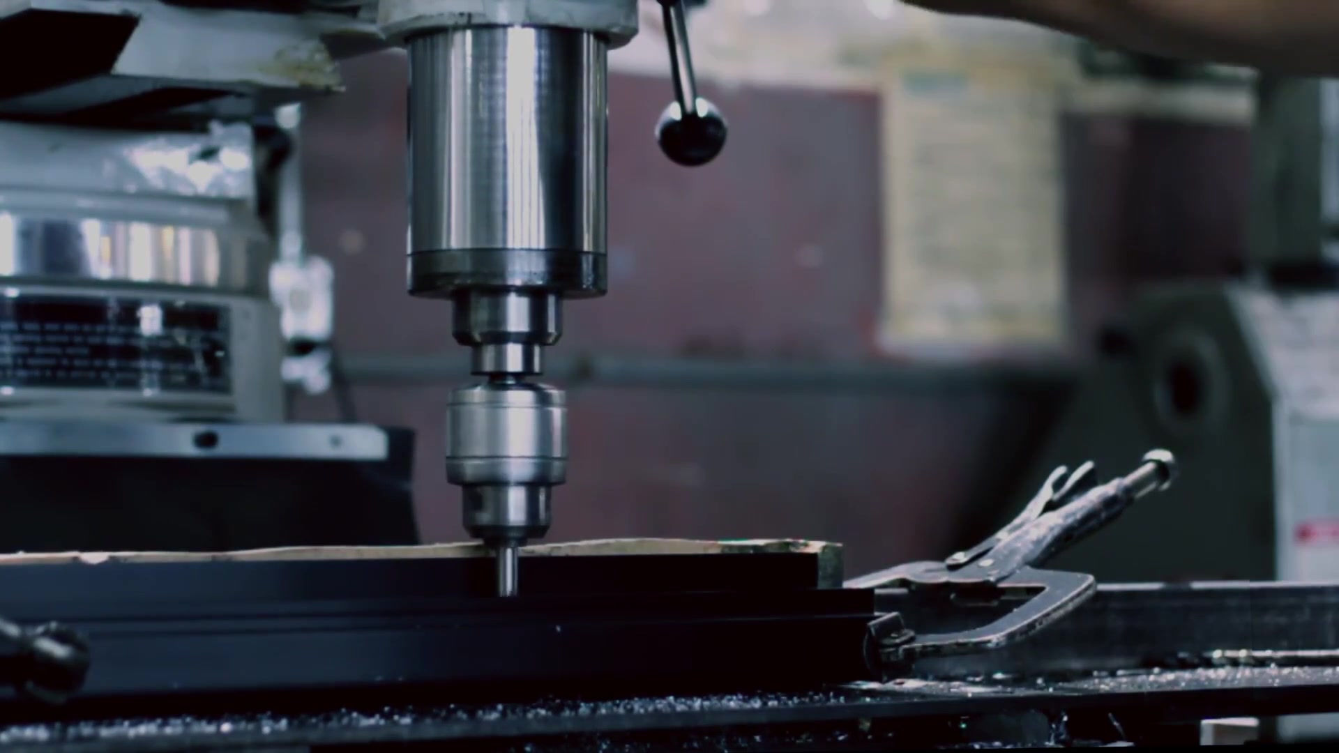
MESOSCALE MANUFACTURING or MESOMANUFACTURING refers to our processes for fabrication of miniature devices such as hearing aids, medical stents, medical valves, mechanical watches and extremely small motors. Mesoscale manufacturing overlaps both macro and micromanufacturing. Miniature lathes, with 1.5 Watt motor and dimensions of 32 x 25 x 30.5 mm and weights of 100 grams have been fabricated using mesoscale manufacturing methods. Using such lathes, brass has been machined to a diameter as small as 60 microns and surface roughnesses in the order of a micron or two. Other such miniature machine tools such as milling machines and presses have also been manufactured using mesomanufacturing.
In MICROELECTRONICS MANUFACTURING we use the same techniques as in micromanufacturing. Our most popular substrates are silicon, and others like gallium arsenide, Indium Phosphide and Germanium are also used. Films/coatings of many types and especially conducting and insulating thin film coatings are used in the fabrication of microelectronic devices and circuits. These devices are usually obtained from multilayers. Insulating layers are generally obtained by oxidation such as SiO2. Dopants (both p and n) type are common and parts of the devices are doped in order to alter their electronic properties and obtain p and n type regions. Using lithography such as ultraviolet, deep or extreme ultraviolet photolithography, or X-ray, electron beam lithography we transfer geometric patterns defining the devices from a photomask/mask to the substrate surfaces. These lithography processes are applied several times in the micromanufacturing of microelectronic chips in order to achieve the required structures in the design. Also etching processes are carried out by which entire films or particular sections of films or substrate are removed. Briefly, by using various deposition, etching and multiple lithographic steps we obtain the multilayer structures on the supporting semiconductor substrates. After the wafers are processed and many circuits are microfabricated on them, the repetitive parts are cut and individual dies are obtained. Each die is thereafter wire bonded, packaged and tested and becomes a commercial microelectronic product. Some more details of microelectronics manufacturing can be found in our submenu, however the subject is very extensive and therefore we encourgae you to contact us in case you need product specific information or more details.
Our MICROFLUIDICS MANUFACTURING operations are aimed at fabrication of devices and systems in which small volumes of fluids are handled. Examples of microfluidic devices are micro-propulsion devices, lab-on-a-chip systems, micro-thermal devices, inkjet printheads and more. In microfluidics we have to deal with the precise control and manipulation of fluids constrained to sub-milimeter regions. Fluids are moved, mixed, separated and processed. In microfluidic systems fluids are moved and controlled either actively using tiny micropumps and microvalves and the like or passively taking advantage of capillary forces. With lab-on-a-chip systems, processes which are normally carried out in a lab are miniaturized on a single chip in order to enhance efficiency and mobility as well as reduce sample and reagent volumes. We have the capability to design microfluidic devices for you and offer microfluidics prototyping & micromanufacturing custom tailored for your applications.
Another promising field in microfabrication is MICRO-OPTICS MANUFACTURING. Micro-optics allows the manipulation of light and the management of photons with micron and sub-micron scale structures and components. Micro-optics allows us to interface the macroscopic world we live in with the microscopic world of opto- and nano-electronic data processing. Micro-optical components and subsystems find widespread applications in the following fields:
Information technology: In micro-displays, micro-projectors, optical data storage, micro-cameras, scanners, printers, copiers…etc.
Biomedicine: Minimally-invasive/point of care diagnostics, treatment monitoring, micro-imaging sensors, retinal implants.
Lighting: Systems based on LEDs and other efficient light sources
Safety and Security Systems: Infrared night vision systems for automotive applications, optical fingerprint sensors, retinal scanners.
Optical Communication & Telecommunication: In photonic switches, passive fiber optic components, optical amplifiers, mainframe and personal computer interconnect systems
Smart structures: In optical fiber-based sensing systems and much more
As the most diverse engineering integration provider we pride ourselves with our capability to provide a solution for almost any consulting, engineering, reverse engineering, rapid prototyping, product development, manufacturing, fabrication and assembly needs.
After micromanufacturing our components, very often we need to continue with MICRO ASSEMBLY & PACKAGING. This involves processes such as die attachment, wire bonding, connectorization, hermetic sealing of packages, probing, testing of packaged products for environmental reliability…etc. After micromanufacturing devices on a die, we attach the die to a more rugged foundation to ensure reliability. Frequently we use special epoxy cements or eutectic alloys to bond the die to its package. After the chip or die is bonded to its substrate, we connect it electrically to the package leads using wire bonding. One method is to use very thin gold wires from the package leads to bonding pads located around the perimeter of the die. Lastly we need to do the final packaging of the connected circuit. Depending on the application and operating environment, a variety of standard and custom manufactured packages are available for micromanufactured electronic, electro-optic, and microelectromechanical devices.
Another micromanufacturing technique we use is SOFT LITHOGRAPHY, a term used for a number of processes for pattern transfer. A master mold is needed in all cases and is microfabricated using standard lithography methods. Using the master mold, we produce an elastomeric pattern / stamp. One variation of soft lithography is “microcontact printing”. The elastomer stamp is coated with an ink and pressed against a surface. The pattern peaks contact the surface and a thin layer of about 1 monolayer of the ink is transfered. This thin film monolayer acts as the mask for selective wet etching. A second variation is “microtransfer molding”, in which the recesses of the elastomer mold are filled with liquid polymer precursor and pushed against a surface. Once the polymer cures, we peel off the mold, leaving behind the desired pattern. Lastly a third variation is “micromolding in capillaries”, where the elastomer stamp pattern consists of channels that use capillary forces to wick a liquid polymer into the stamp from its side. Basically, a small amount of the liquid polymer is placed adjacent to the capillary channels and the capillary forces pull the liquid into the channels. Excess liquid polymer is removed and polymer inside the channels is allowed to cure. The stamp mold is peeled off and the product is ready. You can find more details about our soft lithography micromanufacturing techniques by clicking on the related submenu on the side of this page.
If you are mostly interested in our engineering and research & development capabilities instead of manufacturing capabilities, then we invite you to also visit our engineering website