

Global Custom Manufacturer, Integrator, Consolidator, Outsourcing Partner for a Wide Variety of Products & Services.
We are your one-stop source for manufacturing, fabrication, engineering, consolidation, integration, outsourcing of custom manufactured and off-shelf products & services. We also private label / white label your products with your brand name if you wish.
Choose your Language
-
Custom Manufacturing of Parts, Components, Assemblies, Finished Products, Machines and Industrial Equipment
-
Domestic & Global Contract Manufacturing
-
Manufacturing Outsourcing
-
Domestic, Global Procurement of Industrial Products
-
Private labeling / White Labeling your Products with your Brand Name
-
Product Finding & Locating Services
-
Global Design and Channel Partnership
-
Engineering Integration
-
Engineering Services
-
Global Consolidation, Warehousing, Logistics
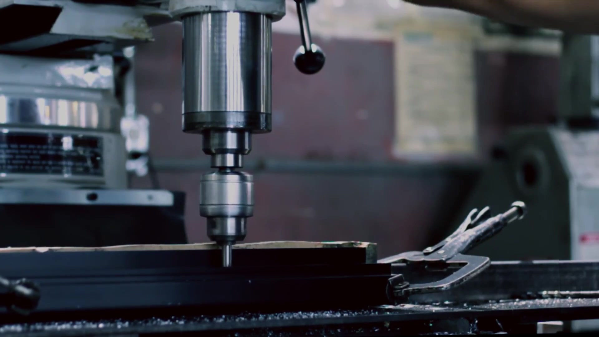
Microelectronics & Semiconductor Manufacturing and Fabrication

Many of our nanomanufacturing, micromanufacturing and mesomanufacturing techniques and processes explained under the other menus can be used for MICROELECTRONICS MANUFACTURING too. However due to the importance of microelectronics in our products, we will concentrate on the subject specific applications of these processes here. Microelectronics related processes are also widely referred to as SEMICONDUCTOR FABRICATION processes. Our semiconductor engineering design and fabrication services include:
- FPGA board design, development and programming
- Microelectronics foundry services: Design, prototyping and manufacturing, third-party services
- Semiconductor wafer preparation: Dicing, backgrinding, thinning, reticle placement, die sorting, pick and place, inspection
- Microelectronic package design and fabrication: Both off-shelf and custom design and fabrication
- Semiconductor IC assembly & packaging & test: Die, wire and chip bonding, encapsulation, assembly, marking and branding
- Lead frames for semiconductor devices: Both off-shelf and custom design and fabrication
- Design and fabrication of heat sinks for microelectronics: Both off-shelf and custom design and fabrication
- Sensor & actuator design and fabrication: Both off-shelf and custom design and fabrication
- Optoelectronic & photonic circuits design and fabrication
Let us examine the microelectronics and semiconductor fabrication and test technologies in more detail so you can better understand the services and products we are offering.
FPGA Board Design & Development and Programming: Field-programmable gate arrays (FPGAs) are reprogrammable silicon chips. Contrary to processors that you find in personal computers, programming an FPGA rewires the chip itself to implement user’s functionality rather than running a software application. Using prebuilt logic blocks and programmable routing resources, FPGA chips can be configured to implement custom hardware functionality without using a breadboard and soldering iron. Digital computing tasks are carried out in software and compiled down to a configuration file or bitstream that contains information on how the components should be wired together. FPGAs can be used to implement any logical function that an ASIC could perform and are completely reconfigurable and can be given a completely different “personality” by recompiling a different circuit configuration. FPGAs combine the best parts of application-specific integrated circuits (ASICs) and processor-based systems. These benefits include the following:
• Faster I/O response times and specialized functionality
• Exceeding the computing power of digital signal processors (DSPs)
• Rapid prototyping and verification without the fabrication process of custom ASIC
• Implementation of custom functionality with the reliability of dedicated deterministic hardware
• Field-upgradable eliminating the expense of custom ASIC re-design and maintenance
FPGAs provide speed and reliability, without requiring high volumes to justify the large upfront expense of custom ASIC design. Reprogrammable silicon also has the same flexibility of software running on processor-based systems, and it is not limited by the number of processing cores available. Unlike processors, FPGAs are truly parallel in nature, so different processing operations do not have to compete for the same resources. Each independent processing task is assigned to a dedicated section of the chip, and can function autonomously without any influence from other logic blocks. As a result, the performance of one part of the application is not affected when more processing is added on. Some FPGAs have analog features in addition to digital functions. Some common analog features are programmable slew rate and drive strength on each output pin, allowing the engineer to set slow rates on lightly loaded pins that would otherwise ring or couple unacceptably, and to set stronger, faster rates on heavily loaded pins on high-speed channels that would otherwise run too slowly. Another relatively common analog feature is differential comparators on input pins designed to be connected to differential signaling channels. Some mixed signal FPGAs have integrated peripheral analog-to-digital converters (ADCs) and digital-to-analog converters (DACs) with analog signal conditioning blocks that allow them to operate as a system-on-a-chip.
Briefly, the top 5 benefits of FPGA chips are:
1. Good Performance
2. Short Time to Market
3. Low Cost
4. High Reliability
5. Long-Term Maintenance Capability
Good Performance – With their capability of accommodating parallel processing, FPGAs have better computing power than digital signal processors (DSPs) and do not require sequential execution as DSPs and can accomplish more per clock cycles. Controlling inputs and outputs (I/O) at the hardware level provides faster response times and specialized functionality to closely match application requirements.
Short Time to market - FPGAs offer flexibility and rapid prototyping capabilities and thus shorter time-to-market. Our customers can test an idea or concept and verify it in hardware without going through the long and expensive fabrication process of custom ASIC design. We can implement incremental changes and iterate on an FPGA design within hours instead of weeks. Commercial off-the-shelf hardware is also available with different types of I/O already connected to a user-programmable FPGA chip. The growing availability of high-level software tools offer valuable IP cores (prebuilt functions) for advanced control and signal processing.
Low Cost—The nonrecurring engineering (NRE) expenses of custom ASIC designs exceed that of FPGA-based hardware solutions. The large initial investment in ASICs can be justified for OEMs producing many chips per year, however many end users need custom hardware functionality for the many systems in development. Our programmable silicon FPGA offers you something with no fabrication costs or long lead times for assembly. System requirements frequently change over time, and the cost of making incremental changes to FPGA designs is negligible when compared to the large expense of respinning an ASIC.
High Reliability - Software tools provide the programming environment and FPGA circuitry is a true implementation of program execution. Processor-based systems generally involve multiple layers of abstraction to help task scheduling and share resources among multiple processes. The driver layer controls hardware resources and the OS manages memory and processor bandwidth. For any given processor core, only one instruction can execute at a time, and processor-based systems are continually at risk of time-critical tasks preempting one another. FPGAs, do not use OSs, pose minimum reliability concerns with their true parallel execution and deterministic hardware dedicated to every task.
Long-term Maintenance Capability - FPGA chips are field-upgradable and do not require the time and cost involved with redesigning ASIC. Digital communication protocols, for example, have specifications that can change over time, and ASIC-based interfaces may cause maintenance and forward-compatibility challenges. To the contrary, reconfigurable FPGA chips can keep up with potentially necessary future modifications. As products and systems mature, our customers can make functional enhancements without spending time redesigning hardware and modifying the board layouts.
Microelectronics Foundry Services: Our microelectronics foundry services include design, prototyping and manufacturing, third-party services. We provide our customers with assistance throughout the entire product development cycle - from design support to prototyping and manufacturing support of semiconductor chips. Our objective in design support services is to enable a first-time right approach for digital, analog, and mixed-signal designs of semiconductor devices. For example, MEMS specific simulation tools are available. Fabs that can handle 6 and 8 inch wafers for integrated CMOS and MEMS are at your service. We offer our clients design support for all major electronic design automation (EDA) platforms, supplying correct models, process design kits (PDK), analog and digital libraries, and design for manufacturing (DFM) support. We offer two prototyping options for all technologies: the Multi Product Wafer (MPW) service, where several devices are processed in parallel on one wafer, and the Multi Level Mask (MLM) service with four mask levels drawn on the same reticle. These are more economical than the full mask set. The MLM service is highly flexible compared to the fixed dates of the MPW service. Companies may prefer outsourcing semiconductor products to a microelectronics foundry for a number of reasons including the need for a second source, using internal resources for other products and services, willingness to go fabless and decrease risk and burden of running a semiconductor fab…etc. AGS-TECH offers open-platform microelectronics fabrication processes that can be scaled down for small wafer runs as well as mass manufacturing. Under certain circumstances, your existing microelectronics or MEMS fabrication tools or complete tool sets can be transferred as consigned tools or sold tools from your fab into our fab site, or your existing microelectronics and MEMS products can be redesigned using open platform process technologies and ported to a process available at our fab. This is faster and more economical than a custom technology transfer. If desired however customer’s existing microelectronics / MEMS fabrication processes may be transferred.
Semiconductor Wafer Preparation: If desired by customers after wafers are microfabricated, we carry out dicing, backgrinding, thinning, reticle placement, die sorting, pick and place, inspection operations on semiconductor wafers. Semiconductor wafer processing involves metrology in between the various processing steps. For example, thin film test methods based on ellipsometry or reflectometry, are used to tightly control the thickness of gate oxide, as well as the thickness, refractive index and extinction coefficient of photoresist and other coatings. We use semiconductor wafer test equipment to verify that the wafers haven't been damaged by previous processing steps up until testing. Once the front-end processes have been completed, the semiconductor microelectronic devices are subjected to a variety of electrical tests to determine if they function properly. We refer to the proportion of microelectronics devices on the wafer found to perform properly as the “yield”. Testing of microelectronics chips on the wafer are carried out with an electronic tester that presses tiny probes against the semiconductor chip. The automated machine marks each bad microelectronics chip with a drop of dye. Wafer test data is logged into a central computer database and semiconductor chips are sorted into virtual bins according to predetermined test limits. The resulting binning data can be graphed, or logged, on a wafer map to trace manufacturing defects and mark bad chips. This map can also be used during wafer assembly and packaging. In final testing, microelectronics chips are tested again after packaging, because bond wires may be missing, or analog performance may be altered by the package. After a semiconductor wafer is tested, it is typically reduced in thickness before the wafer is scored and then broken into individual dies. This process is called semiconductor wafer dicing. We use automated pick-and-place machines specially manufactured for microelectronics industry to sort out the good and bad semiconductor dies. Only the good, unmarked semiconductor chips are packaged. Next, in the microelectronics plastic or ceramic packaging process we mount the semiconductor die, connect the die pads to the pins on the package, and seal the die. Tiny gold wires are used to connect the pads to the pins using automated machines. Chip scale package (CSP) is another microelectronics packaging technology. A plastic dual in-line package (DIP), like most packages, is multiple times larger than the actual semiconductor die placed inside, whereas CSP chips are nearly the size of the microelectronics die; and a CSP can be constructed for each die before the semiconductor wafer is diced. The packaged microelectronics chips are re-tested to make sure that they are not damaged during packaging and that the die-to-pin interconnect process was completed correctly. Using lasers we then etch the chip names and numbers on the package.
Microelectronic Package Design and Fabrication: We offer both off-shelf and custom design and fabrication of microelectronic packages. As part of this service, modeling and simulation of microelectronic packages is also carried out. Modeling and simulation ensures virtual Design of Experiments (DoE) to achieve the optimal solution, rather than testing packages on the field. This reduces the cost and production time, especially for new product development in microelectronics. This work also gives us the opportunity to explain our customers how the assembly, reliability and testing will impact their microelectronic products. The primary objective of microelectronic packaging is to design an electronic system that will satisfy the requirements for a particular application at a reasonable cost. Because of the many options available to interconnect and house a microelectronics system, the choice of a packaging technology for a given application needs expert evaluation. Selection criteria for microelectronics packages may include some of the following technology drivers:
-Wireability
-Yield
-Cost
-Heat dissipation properties
-Electromagnetic shielding performance
-Mechanical toughness
-Reliability
These design considerations for microelectronics packages affect speed, functionality, junction temperatures, volume, weight and more. The primary goal is to select the most cost-effective yet reliable interconnection technology. We use sophisticated analysis methods and software to design microelectronics packages. Microelectronics packaging deals with the design of methods for the fabrication of interconnected miniature electronic systems and the reliability of those systems. Specifically, microelectronics packaging involves routing of signals while maintaining signal integrity, distributing ground and power to semiconductor integrated circuits, dispersing dissipated heat while maintaining structural and material integrity, and protecting the circuit from environmental hazards. Generally, methods for packaging microelectronics ICs involve the use of a PWB with connectors that provide the real-world I/Os to an electronic circuit. Traditional microelectronics packaging approaches involve the use of single packages. The main advantage of a single-chip package is the ability to fully test the microelectronics IC before interconnecting it to the underlying substrate. Such packaged semiconductor devices are either through-hole mounted or surface mounted to the PWB. Surface-mounted microelectronics packages do not require via holes to go through the entire board. Instead, surface-mounted microelectronics components can be soldered to both sides of the PWB, enabling higher circuit density. This approach is called surface-mount technology (SMT). The addition of area-array–style packages such as ball-grid arrays (BGAs) and chip-scale packages (CSPs) is making SMT competitive with the highest-density semiconductor microelectronics packaging technologies. A newer packaging technology involves the attachment of more than one semiconductor device onto a high-density interconnection substrate, which is then mounted in a large package, providing both I/O pins and environmental protection. This multichip module (MCM) technology is further characterized by the substrate technologies used to interconnect the attached ICs. MCM-D represents deposited thin film metal and dielectric multilayers. MCM-D substrates have the highest wiring densities of all MCM technologies thanks to the sophisticated semiconductor processing technologies. MCM-C refers to multilayered “ceramic” substrates, fired from stacked alternating layers of screened metal inks and unfired ceramic sheets. Using MCM-C we obtain a moderately dense wiring capacity. MCM-L refers to multilayer substrates made from stacked, metallized PWB “laminates,” that are individually patterned and then laminated. It used to be a low-density interconnect technology, however now MCM-L is quickly approaching the density of MCM-C and MCM-D microelectronics packaging technologies. Direct chip attach (DCA) or chip-on-board (COB) microelectronics packaging technology involves mounting the microelectronics ICs directly to the PWB. A plastic encapsulant, which is “globbed” over the bare IC and then cured, provides environmental protection. Microelectronics ICs can be interconnected to the substrate using either flip-chip, or wire bonding methods. DCA technology is particularly economical for systems that are limited to 10 or fewer semiconductor ICs, since larger numbers of chips can affect system yield and DCA assemblies can be difficult to rework. An advantage common to both the DCA and MCM packaging options is the elimination of the semiconductor IC package interconnection level, which allows closer proximity (shorter signal transmission delays) and reduced lead inductance. The primary disadvantage with both methods is the difficulty in purchasing fully tested microelectronics ICs. Other disadvantages of DCA and MCM-L technologies include poor thermal management thanks to the low thermal conductivity of PWB laminates and a poor coefficient of thermal expansion match between the semiconductor die and the substrate. Solving the thermal expansion mismatch problem requires an interposer substrate such as molybdenum for wire bonded die and an underfill epoxy for flip-chip die. The multichip carrier module (MCCM) combines all the positive aspects of DCA with MCM technology. The MCCM is simply a small MCM on a thin metal carrier that can be bonded or mechanically attached to a PWB. The metal bottom acts as both a heat dissipater and a stress interposer for the MCM substrate. The MCCM has peripheral leads for wire bonding, soldering, or tab bonding to a PWB. Bare semiconductor ICs are protected using a glob-top material. When you contact us, we will discuss your application and requirements to choose the best microelectronics packaging option for you.
Semiconductor IC Assembly & Packaging & Test: As part of our microelectronics fabrication services we offer die, wire and chip bonding, encapsulation, assembly, marking and branding, testing. For a semiconductor chip or integrated microelectronics circuit to function, it needs to be connected to the system that it will control or provide instructions to. Microelectronics IC assembly does provide the connections for power and information transfer between the chip and the system. This is accomplished by connecting the microelectronics chip to a package or directly connecting it to the PCB for these functions. Connections between the chip and the package or printed circuit board (PCB) are via wire bonding, thru-hole or flip chip assembly. We are an industry leader in finding microelectronics IC packaging solutions to meet the complex requirements of the wireless and internet markets. We offer thousands of different package formats and sizes, ranging from traditional leadframe microelectronics IC packages for thru-hole and surface mount, to the latest chip scale (CSP) and ball grid array (BGA) solutions required in high pin count and high density applications. A wide variety of packages are available from stock including CABGA (Chip Array BGA), CQFP, CTBGA (Chip Array Thin Core BGA), CVBGA (Very Thin Chip Array BGA), Flip Chip, LCC, LGA, MQFP, PBGA, PDIP, PLCC, PoP - Package on Package, PoP TMV - Through Mold Via, SOIC / SOJ, SSOP, TQFP, TSOP, WLP (Wafer Level Package)…..etc. Wire bonding using copper, silver or gold are among the popular in microelectronics. Copper (Cu) wire has been a method of connecting silicon semiconductor dies to the microelectronics package terminals. With recent increase in gold (Au) wire cost, copper (Cu) wire is an attractive way to manage overall package cost in microelectronics. It also resembles gold (Au) wire due to its similar electrical properties. Self inductance and self capacitance are almost the same for gold (Au) and copper (Cu) wire with copper (Cu) wire having lower resistivity. In microelectronics applications where resistance due to bond wire can negatively impact circuit performance, using copper (Cu) wire can offer improvement. Copper, Palladium Coated Copper (PCC) and Silver (Ag) alloy wires have emerged as alternatives to gold bond wires due to cost. Copper-based wires are inexpensive and have low electrical resistivity. However, the hardness of copper makes it difficult to use in many applications such as those with fragile bond pad structures. For these applications, Ag-Alloy offers properties similar to those of gold while its cost is similar to that of PCC. Ag-Alloy wire is softer than PCC resulting in lower Al-Splash and lower risk of bond pad damage. Ag-Alloy wire is the best low cost replacement for applications that need die-to-die bonding, waterfall bonding, ultra-fine bond pad pitch and small bond pad openings, ultra low loop height. We provide a complete range of semiconductor testing services including wafer testing, various types of final testing, system level testing, strip testing and complete end-of-line services. We test a variety of semiconductor device types across all of our package families including radio frequency, analog and mixed signal, digital, power management, memory and various combinations such as ASIC, multi chip modules, System-in-Package (SiP), and stacked 3D packaging, sensors and MEMS devices such as accelerometers and pressure sensors. Our test hardware and contacting equipment are suitable for custom package size SiP, dual-sided contacting solutions for Package on Package (PoP), TMV PoP, FusionQuad sockets, multiple-row MicroLeadFrame, Fine-Pitch Copper Pillar. Test equipment and test floors are integrated with CIM / CAM tools, yield analysis and performance monitoring to deliver very high efficiency yield the first time. We offer numerous adaptive microelectronics test processes for our customers and offer distributed test flows for SiP and other complex assembly flows. AGS-TECH provides a full range of test consultation, development and engineering services across your entire semiconductor and microelectronics product lifecycle. We understand the unique markets and testing requirements for SiP, automotive, networking, gaming, graphics, computing, RF / wireless. Semiconductor manufacturing processes require fast and precisely controlled marking solutions. Marking speeds over 1000 characters/second and material penetration depths less than 25 microns are common in semiconductor microelectronics industry using advanced lasers. We are capable of marking mold compounds, wafers, ceramics and more with minimal heat input and perfect repeatability. We use lasers with high accuracy to mark even the smallest parts without damage.
Lead frames for Semiconductor Devices: Both off-shelf and custom design and fabrication are possible. Lead frames are utilized in the semiconductor device assembly processes, and are essentially thin layers of metal that connect the wiring from tiny electrical terminals on the semiconductor microelectronics surface to the large-scale circuitry on electrical devices and PCBs. Lead frames are used in almost all semiconductor microelectronics packages. Most microelectronics IC packages are made by placing the semiconductor silicon chip on a lead frame, then wire bonding the chip to the metal leads of that lead frame, and subsequently covering the microelectronics chip with plastic cover. This simple and relatively low cost microelectronics packaging is still the best solution for many applications. Lead frames are produced in long strips, which allows them to be quickly processed on automated assembly machines, and generally two manufacturing processes are used: photo etching of some sort and stamping. In microelectronics lead frame design often demand is for customized specifications and features, designs that enhance electrical and thermal properties, and specific cycle time requirements. We have in-depth experience of microelectronics lead frame manufacturing for an array of different customers using laser assisted photo etching and stamping.
Design and fabrication of heat sinks for microelectronics: Both off-shelf and custom design and fabrication. With the increase in heat dissipation from microelectronics devices and the reduction in overall form factors, thermal management becomes a more a more important element of electronic product design. The consistency in performance and life expectancy of electronic equipment are inversely related to the component temperature of the equipment. The relationship between the reliability and the operating temperature of a typical silicon semiconductor device shows that a reduction in the temperature corresponds to an exponential increase in the reliability and life expectancy of the device. Therefore, long life and reliable performance of a semiconductor microelectronics component may be achieved by effectively controlling the device operating temperature within the limits set by the designers. Heat sinks are devices that enhance heat dissipation from a hot surface, usually the outer case of a heat generating component, to a cooler ambient such as air. For the following discussions, air is assumed to be the cooling fluid. In most situations, heat transfer across the interface between the solid surface and the coolant air is the least efficient within the system, and the solid-air interface represents the greatest barrier for heat dissipation. A heat sink lowers this barrier mainly by increasing the surface area that is in direct contact with the coolant. This allows more heat to be dissipated and/or lowers the semiconductor device operating temperature. The primary purpose of a heat sink is to maintain the microelectronics device temperature below the maximum allowable temperature specified by the semiconductor device manufacturer.
We can classify heat sinks in terms of manufacturing methods and their shapes. The most common types of air-cooled heat sinks include:
- Stampings: Copper or aluminum sheet metals are stamped into desired shapes. they are used in traditional air cooling of electronic components and offer an economical solution to low density thermal problems. They are suitable for high volume production.
- Extrusion: These heat sinks allow the formation of elaborate two-dimensional shapes capable of dissipating large heat loads. They may be cut, machined, and options added. A cross-cutting will produce omnidirectional, rectangular pin fin heat sinks, and incorporating serrated fins improves the performance by approximately 10 to 20%, but with a slower extrusion rate. Extrusion limits, such as the fin height-to-gap fin thickness, usually dictate the flexibility in design options. Typical fin height-to-gap aspect ratio of up to 6 and a minimum fin thickness of 1.3mm, are attainable with standard extrusion techniques. A 10 to 1 aspect ratio and a fin thickness of 0.8″can be obtained with special die design features. However, as the aspect ratio increases, the extrusion tolerance is compromised.
- Bonded/Fabricated Fins: Most air cooled heat sinks are convection limited, and the overall thermal performance of an air cooled heat sink can often be improved significantly if more surface area can be exposed to the air stream. These high performance heat sinks utilize thermally conductive aluminum-filled epoxy to bond planar fins onto a grooved extrusion base plate. This process allows for a much greater fin height-to-gap aspect ratio of 20 to 40, significantly increasing the cooling capacity without increasing the need for volume.
- Castings: Sand, lost wax and die casting processes for aluminum or copper / bronze are available with or without vacuum assistance. We use this technology for fabrication of high density pin fin heat sinks which provide maximum performance when using impingement cooling.
- Folded Fins: Corrugated sheet metal from aluminum or copper increases surface area and the volumetric performance. The heat sink is then attached to either a base plate or directly to the heating surface via epoxy or brazing. It is not suitable for high profile heat sinks on account of the availability and fin efficiency. Hence, it allows high performance heat sinks to be fabricated.
In selecting an appropriate heat sink meeting the required thermal criteria for your microelectronics applications, we need to examine various parameters that affect not only the heat sink performance itself, but also the overall performance of the system. The choice of a particular type of heat sink in microelectronics depends largely to the thermal budget allowed for the heat sink and external conditions surrounding the heat sink. There is never a single value of thermal resistance assigned to a given heat sink, since the thermal resistance varies with external cooling conditions.
Sensor & Actuator Design and Fabrication: Both off-shelf and custom design and fabrication are available. We offer solutions with ready-to-use processes for inertial sensors, pressure and relative pressure sensors and IR temperature sensor devices. By using our IP blocks for accelerometers, IR and pressure sensors or applying your design according to available specifications and design rules, we can have MEMS based sensor devices delivered to you within weeks. Besides MEMS, other types of sensor and actuator structures can be fabricated.
Optoelectronic & photonic circuits design and fabrication: A photonic or optical integrated circuit (PIC) is a device that integrates multiple photonic functions. It can be resembled to electronic integrated circuits in microelectronics. The major difference between the two is that a photonic integrated circuit provides functionality for information signals imposed on optical wavelengths in the visible spectrum or near infrared 850 nm-1650 nm. Fabrication techniques are similar to those used in microelectronics integrated circuits where photolithography is used to pattern wafers for etching and material deposition. Unlike semiconductor microelectronics where the primary device is the transistor, there is no single dominant device in optoelectronics. Photonic chips include low loss interconnect waveguides, power splitters, optical amplifiers, optical modulators, filters, lasers and detectors. These devices require a variety of different materials and fabrication techniques and therefore it is difficult to realize all of them on a single chip. Our applications of photonic integrated circuits are mainly in the areas of fiber-optic communication, biomedical and photonic computing. Some example optoelectronic products we can design and fabricate for you are LEDs (Light Emitting Diodes), diode lasers, optoelectronic receivers, photodiodes, laser distance modules, customized laser modules and more.